Showing posts with label 8085. Show all posts

Down to the silicon: how the Z80's registers are implemented

The 8-bit Z80 microprocessor is famed for use in many early personal computers such the Osborne 1, TRS-80, and Sinclair ZX Spectrum. The Z80 has an innovative design for its internal registers, with two sets of general-purpose registers. The diagram below shows a highly-magnified photo of the Z80 chip, from the Visual 6502 team. Zooming in on the register file at the right, the transistors that make up the registers are visible (with difficulty). Each register is in a column, with the low bit on top and high bit on the bottom. This article explains the details of the Z80's register structure: its architecture, how it works, and exactly how it is implemented, based on my reverse-engineering of the chip.

The die of the Z80 microprocessor, zooming in on the register file. Each register is stored vertically, with bit 0 and the top and bit 15 at the bottom. At the right, drivers connect the registers to the data buses. At the top, circuitry selects a register.

The die of the Z80 microprocessor, zooming in on the register file. Each register is stored vertically, with bit 0 and the top and bit 15 at the bottom. There are two sets of AF/BC/DE/HL registers. At the right, drivers connect the registers to the data buses. At the top, circuitry selects a register.

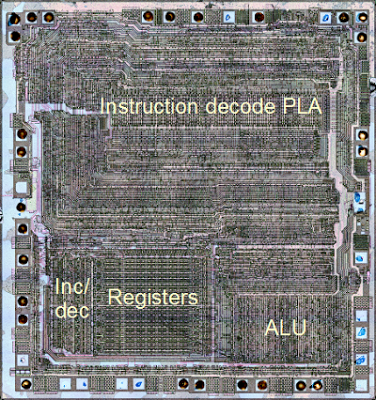
The Z80's architecture is often described with the diagram below, which shows the programmer's model of the chip.[1][2] But as we will see, the Z80's actual register and bus organization differs from this diagram in many ways. For instance, the data bus on the real chip has multiple segments. The diagram shows a separate incrementer for the refresh register (IR), an adder for IX and IY offsets, and a W'Z' register but those don't exist on the real chip. The Z80 shows that the physical implementation of a chip may be very different from how it appears logically.

Programmer's model of Z80 architecture by Appaloosa. Licensed under CC BY-SA 3.0

Programmer's model of Z80 architecture from Wikipedia. Diagram by Appaloosa CC BY-SA 3.0. Original by Rodnay Zaks.

Register overview and layout

The diagram below shows how the Z80's registers are physically arranged on the chip, matching the die photo above. The register file consists of 14 pairs of 8-bit registers. In many cases, a pair of 8-bit registers is treated as a single 16-bit register. The bits are ordered from 0 at the top to 15 at the bottom, so the low-order byte is on the top and the high-order byte is on the bottom.

At the right of the register file are the 8-bit accumulator (A) and 8-bit flag register (F). The accumulator holds the result of arithmetic and logic operations, so it is a very important register. The flag register holds condition flags, for instance indicating a zero value, negative value, overflow value or other conditions.

Note that there are two A registers and two F registers, along with two of BC, DE, and HL. The Z80 is described as having a main register set (AF, BC, DE, and HL) and an alternate register set (A'F', B'C', D'E', and H'L'), and this is how the architecture diagram earlier is drawn. It turns out, though, that this is not how the Z80 is actually implemented. There isn't a main register set and an alternate register set. Instead, there are two of each register and either one can be the main or alternate. This will be explained in more detail below.

Structure of the Z-80's register file. The address is 16 bits wide, while the data buses are 8 bits wide. Gray lines show switches between bus segments.

Structure of the Z-80's register file as implemented on the chip. The address is 16 bits wide, while the data buses are 8 bits wide. Gray lines show switches between bus segments.

To the left of the AF registers are the two general-purpose BC registers. These can be used as 8-bit registers (B or C), or a 16-bit register (BC). Next to them are the similar DE and HL registers. The HL register is often used to reference a location in memory; H holds the high byte of the address, and L holds the low byte. This register structure is based on the earlier 8080 microprocessor. (As will be explained later, DE and HL can swap roles, so these registers should really be labeled H/D and L/E.)

Next to the left are the 16-bit IX and IY index registers. These are used to point to the start of a region in memory, such as a table of data. The 16-bit stack pointer SP is to the left of the index registers. The stack pointer indicates the top of the stack in memory. Data is pushed and popped from the stack, for instance in subroutine calls. To the left of the stack pointer are the 8-bit W and Z registers. As will be discussed below, these are internal registers used for temporary storage and are invisible to the programmer.

Separated from the previous registers is the special-purpose memory refresh register R, which simplifies the hardware when dynamic memory is used.[3] The interrupt page address register I is below R, and is used for interrupt handling. (It provides the high-order byte of an interrupt handler address.)

Finally, at the left is the 16-bit PC (Program Counter), which steps through memory to fetch instructions. Since it is 16 bits, the Z80 can address 64K of memory. Its position next to the incrementer/decrementer is important and will be discussed below.

The Z80's register buses

An important part of the Z80's architecture is how the registers are connected to other parts of the system by various buses. The Z80 is described as having a 16-bit address bus and an 8-bit data bus, but the implementation is more complicated.[3][4] The point of this complexity is to permit multiple register activities as the same time, so the chip can execute faster.

The PC and IR registers are separated from the rest of the registers. As the diagram above shows, these registers are connected to the other registers through a 16-bit bus (thick black line). However, this bus can be connected or disconnected as needed (by pass transistors indicated by the vertical gray line). When disconnected, the PC and R registers can be updated while registers on the right are in use.

The internal register bus connects the PC and IR registers to an incrementer/decrementer/latch circuit. It has multiple uses, but the main purpose is to step the PC from one instruction to the next, and to increment the R register to refresh memory. The resulting address goes to the address pins via the address bus (magenta). I describe the incrementer/decrementer/latch in detail here.

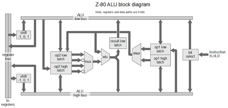
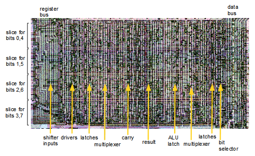
At the right, separate 8-bit data buses connect to the low-order and high-order registers. These two buses can be connected or disconnected as needed. The lower bus (orange) provides access to the ALU (arithmetic logic unit). The upper bus (green) connects to another data bus (red) that accesses the data pins and instruction decoder.

Photo of the Z80 die. The address bus is indicated in purple. The data bus segments are in red, green, and orange.

Photo of the Z80 die. The address bus is indicated in purple. The data bus segments are in red, green, and orange.

Specifying registers in the opcodes

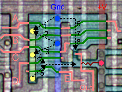
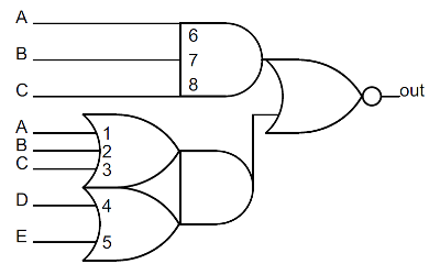
The Z80 uses 8-bit opcodes to specify its instructions, and these instructions are carefully designed to efficiently specify which registers to use. Register instructions normally use three bits to specify the register used: 000=B, 001=C, 010=D, 011=E, 100=H, 101=L, 110=indirect through HL, 111=A.[5] For instance, the ADD instructions have the 8-bit binary values 10000rrr, where the rrr bits specify the register to use as above. Note that in this pattern the two high-order bits specify the register pair, while the low order bit specifies which half of the pair to use; for example 00x is BC, 000 is B, and 001 is C. For instructions operating on a register pair (such as 16-bit increment INC), the opcode uses just the two bits to specify the pair.

By using this structure for opcodes, the instruction decoding logic is simplified since the same circuitry can be reused to select a register or register pair for many different instructions. Instruction decode circuitry located above the register file uses the two bits to select the register pair and then uses the third bit to pick the lower or upper half of the register file.

The register selection bits can be in bits 2-0 of the instruction, for example AND; in bits 5-3 of the instruction, for example DEC (decrement); or in both positions, for example register-to-register LD.[6] To handle this, a multiplexer selects the appropriate group of bits and feeds them into the register select logic. Thus, the same circuit efficiently handles register bits in either position. By designing the instruction set in this way, the Z80 combines the ability to use a large register set with a compact hardware implementation.

Swapping registers through register renaming

The Z80 has several instructions to swap registers or register sets. The EX DE, HL instruction exchanges the DE and HL registers. The EX AF, AF' instruction exchanges the AF and AF' registers. The EXX instruction exchanges the BC, DE, and HL registers with the BC', DE', and HL' registers. These instructions complete very quickly, which raises the question of how multiple 16-bit register values can move around the chip at once.

It turns out that these instructions don't move anything. They just toggle a bit that renames the appropriate registers. For example, consider exchanging the DE and HL registers. If the DE/HL bit is set, an instruction acting on DE uses the first register and an instruction acting on HL uses the second register. If the bit is cleared, a DE instruction uses the second register and a HL instruction uses the first register. Thus, from the programmer's perspective, it looks like the values in the registers have been swapped, but in fact just the meanings/names/labels of the registers have been swapped. Likewise, a bit selects between AF and AF', and a bit selects between BC, DE, HL and the alternates. In all, there are four registers that can be used for DE or HL; physically there aren't separate DE and HL registers.

The hardware to implement register renaming is interesting, using four toggle flip flops.[7] These flip flops are toggled by the appropriate EX and EXX instructions. One flip flop handles AF/AF'. The second flip flop handles BC/DE/HL vs BC'/DE'/HL'. The last two flip flops handle DE vs HL and DE' vs HL'. Note that two flip flops are required since DE and HL can be swapped independently in either register bank.
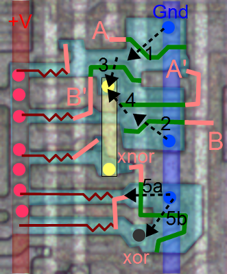
The flags

The flags have a dual existence. The flags are stored inside the register file, but at the start of every instruction,[8] they are copied into latches above the ALU. From this location, the flags can be used and modified by the ALU. (For example, add or shift operations use the carry flag.) At the end of an instruction that affects flags, the flags are copied from the latches back to the register file.

Most of the flags are generated by the ALU (details here). The circuitry to set and use the carry is complicated, since it is used in different ways by shifts and rotates, as well as arithmetic. Conditional operations are another important use of the flags.[9]

The WZ temporary registers

The Z80 (like the 8080 and 8085) has a WZ register pair that is used for temporary storage but is invisible to the programmer. The primary use of WZ is to hold an operand from a two or three byte instruction until it can be used.[10]

The JP (jump) instruction shows why the WZ registers are necessary. This instruction reads a two-byte address following the opcode and jumps to that address. Since the Z80 only reads one byte at a time, the address bytes must be stored somewhere while being read in, before the jump takes place. (If you read the bytes directly into the program counter, you'd end up jumping to a half-old half-new address.) The WZ register pair is used to hold the target address as it gets read in. The CALL (subroutine call) instruction is similar.

Another example is EX (SP), HL which exchanges two bytes on the stack with the HL register. The WZ register pair holds the values at (SP+1) and (SP) temporarily during the exchange.

How the registers are implemented in silicon

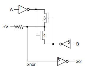
The building block for the registers is a simple circuit to store one bit, consisting of two inverters in a feedback loop. In the diagram below, if the top wire has a 0, the right inverter will output a 1 to the bottom wire. The left inverter will then output a 0 to the top wire, completing the cycle. Thus, the circuit is stable and will "remember" the 0. Likewise, if the top wire is a 1, this will get inverted to a 0 at the bottom wire, and back to a 1 at the top. Thus, this circuit can store either a 0 or a 1, forming a 1-bit memory.[11]

In the Z80, two coupled inverters hold a single bit in the register. This circuit is stable in either the 0 or 1 state.

In the Z80, two coupled inverters hold a single bit in the register. This circuit is stable in either the 0 or 1 state.

How does a value get stored into this inverter pair? Surprisingly, the Z80 just puts stronger signals on the wires, forcing the inverters to take the new values.[12] There's no logic involved, just "might makes right". (In contrast, the 6502 uses an additional transistor in the inverter feedback loop to break the feedback loop when writing a new value.)

To support multiple registers, each register bit is connected to bus lines by two pass transistors. These transistors act as switches that turn on to connect one register to the bus. Each register has a separate bus control signal, connecting the register to the bus when needed. Note that there are two bus lines for each bit - the value and its complement. As explained above, to write a new value to the bit, the new value is forced into the inverters. There are 16 pairs of bus lines running horizontally through the register file, one for each bit.

Each bit of register storage is connected to the bus by pass transistors, allowing the bit to be read or written.

Each bit of register storage is connected to the bus by pass transistors, allowing the bit to be read or written.

Next, to see how an inverter works, the schematic below shows how an inverter is implemented in the Z80. The Z80 uses NMOS transistors, which can be viewed as simple switches. If a 1 is input to the transistor's gate, the switch closes, connecting ground (0) to the output. If a 0 is input to the gate, the switch opens and the output is pulled high (1) by the resistor. Thus, the output is the opposite of the input.[13]

Implementation of an inverter in NMOS.

Implementation of an inverter in NMOS.

Putting this all together - the two inverters and the pass transistors - yields the following schematic for a single bit in the register file. The layout of the schematic matches the actual silicon where the inverters are positioned to minimize the space they take up. The bus lines and ground run horizontally. The control line to connect a register to the buses runs vertically, along with the 5V power line.

Schematic of one bit inside the Z80's register file.

Schematic of one bit inside the Z80's register file.

The diagram below shows the physical implementation of a register bit in the Z80, superimposed on a photo of the die. It's tricky to understand this, but comparing with the schematic above should help. The silicon is in green, the polysilicon is in red, and the metal lines are in blue. Transistors occur where the polysilicon (red) crosses the silicon (green). The X in a box indicates a contact connecting two layers. Note the large area taken up by the resistors (which are formed from depletion-mode transistors). Additional register bits can be seen in the photo, surrounding the bit illustrated.

This diagram shows the layout on silicon of one bit of register storage. Green indicates silicon, red indicates polysilicon, and blue is the metal layer.

This diagram shows the layout on silicon of one bit of register storage. Green indicates silicon, red indicates polysilicon, and blue is the metal layer.

Zooming out, the picture below shows the upper right part of the register file. Each bit consists of a structure like the one above. Each column is a separate register, with a separate control line, and each row is one of the bits. The columns are in groups of two, with the register control lines between the pairs of columns. Zooming out more, the image at the top of the article shows the full register file and its location in the chip. Thus, you can see how the entire register file is built up from simple transistors.

A detail of the Z80 chip, showing part of the register file.

A detail of the Z80 chip, showing part of the register file.

Comparison with the 6502 and 8085

While the Z80's register complement is tiny compared to current processors, it has a solid register set by 1976 standards - about twice as many registers as the 8085 and about four times as many registers as the 6502. Because they share the 8080 heritage, many of the 8085's registers are similar to the Z80, but the Z80 adds the IX and IY index registers, as well as the second set of registers.

The physical structure of the Z80's register file is similar to the 8085 register file. Both use 6-transistor static latches arranged into a 16-bit wide grid. The 8085, however, uses complex differential sense amplifiers to read the values from the registers. The Z80, by contrast, just uses regular gates. I suspect the 8085's designers saved space by making the register transistors as small as possible, requiring extra circuitry to read the weak values on the bus lines.

The 6502, on the other hand, doesn't have a separate register file. Instead, registers are put on the chip where it turns out to be convenient. Since the 6502 has fewer registers, the register circuitry doesn't need to be as optimized and each bit is more complex. The 6502 adds a transistor to each bit so it is clocked, and separate pass transistors for read and write. One consequence is direct register-to-register transfers are possible on the 6502, since the source and destination registers can be distinguished. Instead of a separate incrementer unit, the 6502's program counter is tangled in with the incrementer circuitry.

Conclusion

By looking at the silicon of the Z80 in detail, we can determine exactly how it works. The Z80's register file has more complexity than you'd expect and the hardware implementation is different from published architecture diagrams. By splitting the register file in two, the Z80 runs faster since registers can be updated in parallel. The Z80 includes a WZ register pair for temporary storage that isn't visible to the programmer. The Z80's register storage has many similarities to the 8085, both in the registers provided and their hardware implementation, but is very different from the 6502.

Credits: This couldn't have been done without the Visual 6502 team especially Chris Smith, Ed Spittles, Pavel Zima, Phil Mainwaring, and Julien Oster. All die photos are from the visual 6502 team.

Notes and references

[1] There are many variants of that architecture diagram; the one above is from Wikipedia. The original source of the common Z80 architecture diagram is the book Programming the Z80 by Rodnay Zaks, page 65 (HTML or PDF). The book is an extremely detailed guide to the Z80, down to the instruction cycles. I don't mean to criticize the architecture diagram by pointing out differences between it and the actual silicon. After all, it is a logic-level diagram intended for use by programmers, not a hardware reference. But it is interesting to see the differences between the programmer's view and the hardware implementation.

[2] Zilog's Z80 CPU user manual is a key reference on the instruction set and operation of the Z80, but it doesn't provide any information on the internal architecture.

[3] The Z80's memory refresh feature is described in patent 4332008. Figure 15 in the patent shows the segmented data bus used by the Z80, although it is a mirror image of the actual die.

[4] I wrote more about the data buses in the Z-80 in Why the Z-80's data pins are scrambled.

[5] The bit pattern 110 is an exception to the encoding of registers in instructions, since it refers to a memory location indexed by the HL register pair, rather than a register. Likewise the bit pattern 11x referring to a register pair is also an exception. It can indicate the SP register, for example in 16-bit LD, INC and DEC instructions.

[6] The Z80 specifies registers in instruction bits 0-2 and bits 3-5. This maps cleanly onto octal, but not hexadecimal. One consequence is the opcodes are more logical if you arrange them in octal (like this), instead of hexadecimal (like this). Perhaps the designers of the Z80 were thinking in octal and not hex.

[7] The toggle flip flops are unlike standard flip flops formed from gates. Instead they use pass transistors; this lets it hold the previous state while toggling to avoid oscillation. Because the pass transistor circuits depend on capacitance holding the values, you have to keep the clock running. This is one reason the clock in the Z80 can't stop for more than a couple microseconds. (The CMOS version is different and the clock can stop arbitrarily long.) From looking at the silicon, it appears that these flip flops required some modifications to work reliably, probably to ensure they toggled exactly once.

These flip flops have no reset logic, so it is unpredictable how the registers get assigned on power-up. Since there's no way to tell which register is which, this doesn't matter.

The active DE vs HL flip flop swaps the DE and HL register control lines using pass-gate multiplexers. The main vs alternate register set flip flops direct each AF/BC/DE/HL register control line to one of the two registers in the pair.

[8] Like many processors of its era, the Z80 starts fetching a new instruction before the previous instruction is finished; this is known as fetch/execute overlap. As a result, the flags are actually written from the latches to the register file three cycles into the next instruction (i.e. T3), and the flags are read from the register file into the latches four cycles into the instruction (i.e. T4).

[9] I'll explain briefly how conditional instructions such as jump (JP) work with the flags. Bits 4 and 5 of the opcode select the flag to use (via a multiplexer just to the right of the registers). Bit 3 of the opcode indicates the desired value (clear or set); this bit is XORed with the selected flag's value. The result indicates if the desired condition is satisfied or not, and is fed into the control logic to determine the appropriate action. The JR and DJNZ don't exactly fit the pattern so a couple additional gates adjust their bits to pick the right flags.

[10] For more explanation of the WZ registers, see Programming the Z80, pages 87-91.

[11] The register storage in the Z80 is called "static" memory, since it will store data as long as the circuit has power. In contrast, your computer uses dynamic memory, which will lose data in milliseconds if the data isn't constantly refreshed. The advantage of dynamic memory is it is much simpler (a transistor and a capacitor), and thus each cell is much smaller. (This is how DRAM can fit gigabits onto a single chip.) Another alternative is flash memory, which has the big advantage of keeping its contents while the power is turned off.

[12] If you've built electronic circuits, it may seem dodgy to force the inverters to change values by overpowering the outputs. But this is a standard technique in chips. To understand what happens, remember that in an NMOS circuit, a 0 output is created by a transistor to ground, while a 1 output is made by a much weaker resistor. So if one of the inverters is outputting a 1 and a 0 is connected to the output, the 0 will "win". This will cause the other inverter to immediately switch to 1. At this point, the original inverter will switch to output 0 and the inverter pair is now stable with the new values.

To improve speed, and to prevent a low voltage on the bus from accidentally clearing a bit while reading a register, the bus lines are all precharged to +5 every clock cycle. A low output from an inverter will have no trouble pulling the bus line low, and a high output will leave the bus line high. The precharging is done through transistors in the space between the IR and WZ registers.

[13] One disadvantage of NMOS logic is the pull-up resistors waste power. In addition, the output is fairly slow (by computer standards) to change from 0 to 1 because of the limited current through the resistor. For these, reasons, NMOS has been almost entirely replaced by CMOS logic which instead of resistors uses complementary transistors to pull the output high. (As a result, CMOS uses almost no power except while switching outputs from one state to another. For this reason, CMOS power usage scales up with frequency, which is why CPUs are hitting clock limits - they're too hot to run any faster.)

The Z-80's 16-bit increment/decrement circuit reverse engineered

The 8-bit Z-80 processor was very popular in the late 1970s and early 1980s, powering many personal computers such as the Osborne 1, TRS-80, and Sinclair ZX Spectrum. It has a 16-bit incrementer/decrementer that efficiently updates the program counter and stack pointer, as well as supporting several 16-bit instructions and memory refresh. By reverse engineering detailed die photographs of the Z-80, we can see exactly how this increment/decrement circuit works and discover the interesting optimizations it uses for efficiency.

The Z-80 microprocessor die, showing the main components of the chip.

The Z-80 microprocessor die, showing the main components of the chip.

The increment/decrement circuit in the lower left corner of the chip photograph above. This circuit takes up a significant amount of space on the chip, illustrating its complexity. It is located close to the register file, allowing it to access the registers directly.

The fundamental use for an incrementer is to step the program counter from instruction to instruction as the program executes. Since this happens at least once for every instruction, a fast incrementer is critical to the performance of the chip. For this reason, the incrementer/decrementer is positioned close to the address pins (along the left and bottom of the photograph above). A second key use is to decrement the stack pointer as data is pushed to the stack, and increment the stack pointer as data is popped from the stack. (This may seem backwards, but the stack grows downwards so it is decremented as data is pushed to the stack.)

The incrementer/decrementer in the Z-80 is also used for a variety of other instructions. For example, the INC and DEC instructions allow 16-bit register pairs to be incremented and decremented. The Z-80 includes powerful block copy and compare instructions (LDIR, LDDR, CPIR, CPDR) that can process up to 64K bytes with a single instruction. These instructions use the 16-bit BC register pair as a loop counter, and the decrementer updates this register pair to count the iterations.

One of the innovative features of the Z-80 is that it includes a DRAM refresh feature. Because Dynamic RAM (DRAM) stores data in capacitors instead of flip flops, the data will drain away if not accessed and refreshed every few milliseconds. Early microcomputer memory boards required special refresh hardware to periodically step through the address space and refresh memory. The incrementer is used to update the address in the refresh register R on each instruction. (Current systems still require memory refresh, but it is handled by the DDR memory modules and memory controller).

Architecture

The architecture diagram below provides a simplified view of how the incrementer/decrementer works with the rest of the Z-80. The incrementer is closely associated with the 16-bit address bus. The data bus, on the other hand, is only 8 bits wide. Many of the registers are 8 bits, but can be paired together as 16-bit registers (BC, DE, HL).

A 16-bit latch feeds into the incrementer. This is needed since if a value were read from the PC, incremented, and written back to the PC at the same time a loop would occur. By latching the value, the read and write are done in separate cycles, avoiding instability. On the chip, the latch is between the incrementer and the register file.

The program counter and refresh register are separated from the rest of the registers and coupled closely to the incrementer. This allows the incrementer to be used in parallel with the rest of the Z-80. In particular, for each instruction fetch, the program counter (PC) is written to the address bus and incremented. Then the refresh address is written to the address bus for the refresh cycle, and the R register is incremented. (Note that the interrupt vector register I is in the same register pair as the R register. This explains why the I value is also written to the address bus during refresh.)

This diagram shows how the incrementer/decrementer is used in the Z-80 microprocessor.

This diagram shows how the incrementer/decrementer is used in the Z-80 microprocessor.

One of the interesting features of the Z-80 is a limited form of pipelining: fetch/execute overlap. Usually, the Z-80 fetches an instruction before the previous instruction has finished executing. The architecture above shows how this is possible. Because the PC and R registers are separated from the other registers, the other registers and ALU can continue to operate during the fetch and refresh steps.

The other registers are not entirely separated from the incrementer/decrementer, though. The stack pointer and other registers can communicate via the bus with the incrementer/decrementer when needed. Pass transistors allow this bus connection to be made as needed.

How a simple incrementer/decrementer works

To understand the circuit, it helps to start with a simple incrementer. If you've studied digital circuits, you've probably seen how two bits can be added with a half-adder, and several half-adders can be chained together to implement a simple multi-bit increment circuit.

The circuit below shows a half-adder, which can increment a single bit. The sum of two bits is computed by XOR, and if both bits are 1, there is a carry.

A simple half-adder that can be used to build an incrementer.

A simple half-adder that can be used to build an incrementer.

Chaining together 16 of these half-adder circuits creates a 16-bit incrementer. Each carry-out is connected to the carry-in of the next bit. A 1 value is fed into the initial carry-in to start the incrementing.

This circuit can be converted to a decrement circuit by renaming the carry signal as a borrow signal. If a bit is 0 and borrow is 1, then there must be a borrow from the next higher bit. (This is similar to grade-school decimal subtraction: 101000 - 1 = 100999 in decimal, since you keep borrowing until you hit a nonzero digit.) When decrementing, a 0 bit potentially causes a borrow, the opposite of incrementing, where a 1 bit potentially causes a carry.

The incrementer and decrementer can be combined into a single circuit by adding one more gate. When computing the carry/borrow for decrementing, each bit is flipped. This is accomplished by using an XOR gate with the decrement condition as an input. If decrement is 1, the input bit is flipped. To increment, the decrement input is set to 0 and the bit passes through the XOR gate unchanged.

A half-adder / subtractor that can be used to build an incrementer/decrementer.

A half-adder / subtractor that can be used to build an incrementer/decrementer.

Repeating the above circuit 16 times creates a 16-bit incrementer/decrementer.

Ripple carry: the problem and solutions

While the circuits above are simple, they have a big problem: they are slow. These circuits use what is called "ripple carry", since the carry value ripples through the circuit bit by bit. The consequence is each bit can't be computed until the carry/borrow is available from the previous bit. This propagation delay limits the clock speed of the system, since the final result isn't available until the carry has made it way through the entire circuit. For a 16-bit counter, this delay is significant.

Carry skip

The Z-80 uses two techniques to avoid ripple carry and speed up the incrementer. First, it uses a technique called carry-skip to compute the result and carry for two bits at a time, reducing the propagation delay.

The circuit diagram below shows how two bits at a time can be computed. Both carry values are computed in parallel, rather than the second carry depending on the first. If both input bits are 1 and there is a carry in, then there is a carry from the left bit. By computing this directly, the propagation delay is reduced.

A circuit to increment or decrement two bits at once.

A circuit to increment or decrement two bits at once.

Due to the MOS gates used in the Z-80, NOR and XNOR gates are more practical than AND and XOR gates, so instead of the carry skip circuit above, the similar circuit below is used in the Z-80. The output bits are inverted, but this is not a problem because many of the Z-80's internal buses are inverted. (The Z-80 uses an interesting pass-transistor XNOR gate, described here. The circuit below performs increment/decrement on two bits, and is repeated six times in the Z-80. To simplify the final schematic, the circuit in the dotted box will simply be shown as a box labeled "2-bit inc/dec".

The circuit used in the Z-80 to increment or decrement two bits.

The circuit used in the Z-80 to increment or decrement two bits.

Carry-lookahead

The second technique used by the Z-80 to avoid the ripple carry delay is carry lookahead, which computes some of the carry values directly from the inputs without waiting on the previous carries. If a sequence of bits is all 1's, there will be a carry from the sequence when it is incremented. Conversely, if there is a 0 anywhere in the sequence, any intermediate carry will be "extinguished". (Similarly, all 0's causes a borrow when decrementing.) By feeding the bits into an AND gate, a sequence of all 1's can be detected, and the carry immediately generated. (The Z-80 uses the inverted bits and a NOR gate, but the idea is the same.)

In the Z-80 three lookahead carries are computed. The carry from the lowest 7 bits is computed directly. If these bits are all 1, and there is a carry-in, then there will be a carry out. The second carry lookahead checks bits 7 through 11 in parallel. The third carry lookahead checks bits 12 through 14 in parallel. Thus, the last bit of the result (bit 15) depends on three carry lookahead steps, rather than 15 ripple steps. This reduces the time for the incrementer to complete.

For more information on carry optimization, see this or this discussion of adders.

The Z-80's increment/decrement circuit

The schematic below shows the actual circuit used in the Z-80 to implement the 16-bit incrementer/decrementer, as determined by reverse engineering the silicon. It uses six of the 2-bit inc/dec blocks described earlier in combination with the three carry-lookahead gates.

In the top half of the schematic, the seven low-order bits are incremented/decremented using the circuit block discussed above. In parallel, the carry/borrow from these bits is computed by the large NOR gate on the left.

Bits 7 through 11 are computed using the carry lookahead value, allowing them to be computed without waiting on the low-order bits. In parallel, the carry/borrow out of these bits is computed by the large NOR gate in the middle, and used to compute bits 12 through 14. The last carry lookahead value is computed at the left and used to compute bit 15. Note that the number of carry blocks decreases as the number of carry lookahead gates increases. For example, output 6 depends on three inc/dec blocks and no carry lookahead gates, while output 14 depends on one inc/dec block and two carry lookahead gates. If the inc/dec blocks and carry lookahead gates require approximately the same time, then the output bits will be ready at approximately the same time.

Schematic of the incrementer/decrementer circuit in the Z-80 microprocessor.

Schematic of the incrementer/decrementer circuit in the Z-80 microprocessor.

The image below shows what the incrementer/decrementer looks like physically, zooming in on the die photograph at the top of the article. The layout on the chip is slightly different from the schematic above. On the chip, the bits are arranged vertically with the low-order bit on top and the high-order bit on the bottom.

The image is a composite: the upper half is from the Z-80 die photograph, while the lower half shows the chip layers as tediously redrawn by the Visual 6502 team for analysis. You can see 8 horizontal "slices" of circuitry from top to bottom, since the bits are processed two at a time. The vertical metal wires are most visible (white in the photograph, blue in the layer drawing). These wires provide power, ground, control signals, and collect the lookahead carry from multiple bits. The polysilicon wires are reddish-orange in the layer diagram, while the diffused silicon is green. Transistors result where the two cross. If you look closely, you can see diagonal orange polysilicon wires about halfway across; these connect the carry-out from one bit to carry-in of the next.

The increment/decrement circuit in the Z-80 microprocessor. Top is the die photograph. Bottom is the layer drawing.

The increment/decrement circuit in the Z-80 microprocessor. Top is the die photograph. Bottom is the layer drawing.

Incrementing the refresh register

The refresh register R and interrupt vector I form a 16-bit pair. The refresh register gets incremented on every memory refresh cycle, but why doesn't the I register get incremented too? This would be a big problem since the value in the I register would get corrupted. The answer is the refresh input into the first carry lookahead gate in the schematic. During a refresh operation, a 1 value is fed into the gate here. This forces the carry to 0, stopping the increment at bit 6, leaving the I register unchanged (along with the top bit of the R register).

You might wonder why only 7 bits of the 8-bit refresh register get incremented. The explanation is that dynamic RAM chips store values in a square matrix. For refresh, only the row address needs to be updated, and all memory values in that row will be refreshed at once. When the Z-80 was introduced, 16K memory chips were popular. Since they held 2^14 bits, they had 7 row address bits and 7 column address bits. Thus, a 7 bit refresh value matched their need. Unfortunately, this rapidly became obsolete with the introduction of 64K memory chips that required 8 refresh bits. [Edit: it's a bit more complicated and depends on the specific chips. See the comments.] Some later chips based on the Z-80, such as the NSC800 had an 8-bit refresh to support these chips.

The non-increment feature

One unexpected feature of the Z-80's incrementer is that it can pass the value through unchanged. If the carry-in to the incrementer/decrementer is set to 0, no action will take place. This seems pointless, but it actually useful since it allows a 16-bit value to be latched and then read back unchanged. In effect, this provides a 16-bit temporary register. The Z-80 uses this action for EX (SP), HL, LD SP, HL, and the associated IX and IY versions. For the LD SP, HL, first HL is loaded into the incrementer latch. Then the unincremented value is stored in the SP register.

The EX (SP), HL is more complex, but uses the latch in a similar way. First the values at (SP+1) and (SP) are read into the WZ temporary register. Next the HL value is written to memory. Finally, WZ is loaded into the incrementer latch and then stored in HL.

You might wonder why values aren't copied between two registers directly. This is due to the structure of the register cells: they do not have separate load and store lines. Instead when a register is connected to the internal register bus, it will be overwritten if another value is on the bus, and otherwise it can be read. Even a simple register-to-register copy such as LD A,B cannot happen directly, but copy the data via the ALU. Since the Z-80's ALU is 4 bits wide, copying a 16-bit value would take at least 4 cycles and be slow. Thus, copying a 16-bit value via the incrementer latch is faster than using the WZ temporary registers.

One timing consequence of using the incrementer latch for 16-bit register-to-register transfers is that it cannot be overlapped with the instruction fetch. Many Z-80 instructions are pipelined and don't finish until several cycles into the next instruction, since register and ALU operations can take place while the Z-80 is fetching the next instruction from memory. However, the PC uses the incrementer during instruction fetch to advance to the next instruction. Thus, any transfer using the incrementer latch must finish before the next instruction starts.

The 0x0001 detector

Another unexpected feature of the incrementer/decrementer is it has a 16-input gate to test if the input is 0x0001 (not shown on the schematic). Why check for 1 and not zero? This circuit is used for the block transfer and search instructions mentioned earlier (LDIR, LDDR, CPIR, CPDR). These operations repeat a transfer or compare multiple times, decrementing the BC register until it reaches zero. But instead of checking for 0 after the decrement, the Z-80 checks if BC register is 1 before the decrement; this works out the same, but gives the Z-80 more time to detect the end of the loop and wrap up instruction execution.

No flags

Unlike the ALU, the incrementer/decrementer doesn't compute parity, negative, carry, or zero values. This is why the 16-bit increment/decrement instructions don't update the status flags.

Comparison with the 6502 and 8085

The 6502 has a 16-bit incrementer, but it is part of the program counter circuit. The 6502 only provides an incrementer, not a decrementer, as the PC doesn't need to be decremented. The other registers are 8 bits, so they don't need a 16-bit incrementer, but use the ALU to be incremented or decremented. (See the 6502 architecture diagram.) The 6502's incrementer uses a couple tricks for efficiency. It uses carry lookahead: the carry from the lowest 8 bits is computed in parallel, as is the carry from the next 4 bits. Alternating bits use a slightly different circuit to avoid inverters in the carry path, slightly reducing the propagation delay.

I've examined the 8085's register file and incrementer in detail. The incrementer/decrementer is implemented by a chain of half-adders with ripple carry. The 8085 has controls to select increment or decrement, similar to the Z-80. The 8085 also includes a feature to increment by two, which speeds up conditional jumps. As in the 6502, an optimization in the 8085 is that alternating bits are implemented with different circuits and the carry out of even bits is inverted. This avoids the inverters that would otherwise be needed to flip the carry back to its regular state. The 8085 uses the carry out from the incrementer to compute the undocumented K flag value.

Conclusion

Looking at the actual circuit for the incrementer/decrementer in the Z-80 shows the performance optimizations in a real chip, compared to a simple incrementer. The 6502 and 8085 also optimize this circuit, but in different ways. In addition, examining the circuitry sheds light on how some operations are implemented in the Z-80, as well as the way memory refresh was handled.

Credits: This couldn't have been done without the Visual 6502 team especially Pavel Zima, Chris Smith, Ed Spittles, Phil Mainwaring, and Julien Oster.

The Z-80 has a 4-bit ALU. Here's how it works.

The 8-bit Z-80 processor is famed for use in many early personal computers such the Osborne 1, TRS-80, and Sinclair ZX Spectrum, and it is still used in embedded systems and TI graphing calculators. I had always assumed that the ALU (arithmetic-logic unit) in the Z-80 was 8 bits wide, like just about every other 8-bit processor. But while reverse-engineering the Z-80, I was shocked to discover the ALU is only 4 bits wide! The founders of Zilog mentioned the 4-bit ALU in a very interesting discussion at the Computer History Museum, so it's not exactly a secret, but it's not well-known either.

I have been reverse-engineering the Z-80 processor using images from the Visual 6502 team. The image below shows the overall structure of the Z-80 chip and the location of the ALU. The remainder of this article dives into the details of the ALU: its architecture, how it works, and exactly how it is implemented.

I've created the following block diagram to give an overview of the structure of the Z-80's ALU. Unlike Z-80 block diagrams published elsewhere, this block diagram is based on the actual silicon. The ALU consists of 4 single-bit units that are stacked to form a 4-bit ALU. At the left of the diagram, the register bus provides the ALU's connection to the register file and the rest of the CPU.

The operation of the ALU starts by loading two 8-bit operands from registers into internal latches. The ALU does a computation on the low 4 bits of the operands and stores the result internally in latches. Next the ALU processes the high 4 bits of the operands. Finally, the ALU writes the 8 bits of result (the 4 low bits from the latch, and the 4 high bits just computed) back to the registers. Thus, by doing two computation cycles, the ALU is able to process a full 8 bits of data. ("Full 8 bits" may not sound like much if you're reading this on a 64-bit processor, but it was plenty at the time.)

As the block diagram shows, the ALU has two internal 4-bit buses connected to the 8-bit register bus: the low bus provides access to bits 0, 1, 2, and 3 of registers, while the high bus provides access to bits 4, 5, 6, and 7. The ALU uses latches to store the operands until it can use them. The op1 latches hold the first operand, and the op2 latches hold the second operand. Each operand has 4 bits of low latch and 4 bits of high latch, to store 8 bits.

Multiplexers select which data is used for the computation. The op1 latches are connected to a multiplexer that selects either the low or high four bits. The op2 latches are connected to a multiplexer that selects either the low or high four bits, as well as selecting either the value or the inverted value. The inverted value is used for subtraction, negation, and comparison.

The two operands go to the "alu core", which performs the desired operation: addition, logical AND, logical OR, or logical XOR. The ALU first performs one computation on the low bits, storing the 4-bit result into the result low latch. The ALU then performs a second computation on the high bits, writing the latched low result and the freshly-computed high bits back to the bus. The carry from the first computation is used in the second computation if needed.

The Z-80 provides extensive bit-addressed operations, allowing a single bit in a byte to be set, reset, or tested. In a bit-addressed operation, bits 5, 4, and 3 of the instruction select which of the 8 bits to use. On the far right of the ALU block diagram is the bit select circuit that support these operations. In this circuit, simple logic gates select one of eight bits based on the instruction. The 8-bit result is written to the ALU bus, where it is used for the bit-addressed operation. Thus, decoding this part of an instruction happens right at the ALU, rather than in the regular instruction decode logic.

The Z-80's shift circuitry is interesting. The 6502 and 8085 have an additional ALU operation for shift right, and perform shift left by adding the number to itself. The Z-80 in comparison performs a shift while loading a value into the ALU. While the Z-80 reads a value from the register bus, the shift circuit selects which lines from the register bus to use. The circuit loads the value unchanged, shifted left one bit, or shifted right one bit. Values shifted in to bit 0 and 7 are handled separately, since they depend on the specific instruction.

The block diagram also shows a path from the low bus to the high op2 latch, and from the high bus to the low op1 latch. These are for the 4-bit BCD shifts RRD and RLD, which rotate a 4-bit digit in the accumulator with two digits in memory.

Not shown in the block diagram are the simple circuits to compute parity, test for zero, and check if a 4-bit value is less than 10. These values are used to set the condition flags.

The silicon that implements the ALU

The image above zooms in on the ALU region of the Z-80 chip. The four horizontal "slices" are visible. The organization of each slice approximately matches the block diagram. The register bus is visible on the left, running vertically with the shifter inputs sticking out from the ALU like "fingers" to obtain the desired bits. The data bus is visible on the right, also running vertically. The horizontal ALU low and ALU high lines are visible at the top and bottom of each slice. The yellow arrows show the locations of some ALU components in one of the slices, but the individual circuits of the ALU are not distinguishable at this scale. In a separate article, I zoom in to some individual gates in the ALU and show how they work: Reverse-engineering the Z-80: the silicon for two interesting gates explained.

The ALU's core computation circuit

The silicon that implements one bit of ALU processing

The heart of each bit of the ALU is a circuit that computes the sum, AND, OR, or XOR for two one-bit operands. Zooming in shows the silicon that implements this circuit; at this scale the transistors and connections that make up the gates are visible. Power, ground, and the control lines are the vertical metal stripes. The shiny horizontal bands are polysilicon "wires" which form the connections in the circuit as well as the transistors. I know this looks like mysterious gray lines, but by examining it methodically, you can figure out the underlying circuit. (For details on how to figure out the logic from this silicon, see my article on the Z-80's gates.) The circuit is shown in the schematic below.

The Z-80 ALU circuit that computes one bit

This circuit takes two operands (op1 and op2), and a carry in. It performs an operation (selected by control lines R, S, and V) and generates an internal carry, a carry-out, and the result.

ALU computation logic in detail

The first step is the "carry computation", which is done by one big multi-level gate. It takes the two operand bits (op1 and op2) and the carry in, and computes the (complemented) internal carry that results from adding op1 plus op2 plus carry-in. There are just two ways this sum can cause a carry: if op1 and op2 are both 1 (bottom AND gate); or if there's a carry-in and at least one of the operands is a 1 (top gates). These two possibilities are combined in the NOR gate to yield the (complemented) internal carry. The internal carry is inverted by the NOR gate at the bottom to yield the carry out, which is the carry in for the next bit. There are a couple control lines that complicate carry generation slightly. If S is 1, the internal carry will be forced to 0. If R is 1, the carry out will be forced to 0 (and thus the carry in for the next bit).

The multi-level result computation gate is interesting as it computes the SUM, XOR, AND or OR. It takes some work to step through the different cases, but if anyone wants the details:

  • SUM: If R is 0, S is 0, and V is 0, then the circuit generates the 1's bit of op1 plus op2 plus carry-in, i.e. op1 xor op2 xor carry-in. To see this, the output is 1 if all three of op1, op2, and carry-in are set, or if at least one is set and there's no internal carry (i.e. exactly one is set).
  • XOR: If R is 1, S is 0, and V is 0, then the circuit generates op1 xor op2 To see this, note that this is like the previous case except carry-in is 0 because of R.
  • AND: If R is 0, S is 1, and V is 0, then the circuit generates op1 and op2. To see this, first note the internal carry is forced to 0, so the lower AND gate can never be active. The carry-in is forced to 1, so the result is generated by the upper AND gate.
  • OR: If R is 1, S is 1, and V is 1, then the circuit generates op1 or op2. The internal carry is forced to 0 by S and the the carry-out (carry-in) is forced to 0 by R. Thus, the top AND gate is disabled, and the 3-input OR gate controls the result.

Believe it or not, this is conceptually a lot simpler than the 8085's ALU, which I described in detail earlier. It's harder to understand, though, then the 6502's ALU, which uses simple gates to compute the AND, OR, SUM, and XOR in parallel, and then selects the desired result with pass transistors.

Conclusion

The Z-80's ALU is significantly different from the 6502 or 8085's ALU. The biggest difference is the 6502 and 8085 use 8-bit ALUs, while the Z-80 uses a 4-bit ALU. The Z-80 supports bit-addressed operations, which the 6502 and 8085 do not. The Z-80's BCD support is more advanced than the 8085's decimal adjust, since the Z-80 handles addition and subtraction, while the 8085 only handles addition. But the 6502 has more advanced BCD support with a decimal mode flag and fast, patented BCD logic.

If you've designed an ALU as part of a college class, it's interesting to compare an "academic" ALU with the highly-optimized ALU used in a real chip. It's interesting to see the short-cuts and tradeoffs that real chips use.

I've created a more detailed schematic of the Z-80 ALU that expands on the block diagram and the core schematic above and shows the gates and transistors that make up the ALU.

I hope this exploration into the Z-80 has convinced you that even with a 4-bit ALU, the Z-80 could still do 8-bit operations. You didn't get ripped off on your old TRS-80.

Credits: This couldn't have been done without the Visual 6502 team especially Chris Smith, Ed Spittles, Pavel Zima, Phil Mainwaring, and Julien Oster.

Reverse-engineering the Z-80: the silicon for two interesting gates explained

I've been reverse-engineering the Z-80 processor, using images from the Visual 6502 team. One interesting thing about the Z-80's silicon is it uses complex gates with multiple inputs and multiple levels of logic. It also implements an XOR gate with an unusual pass-transistor circuit. I thought it would be interesting to examine these gates at the silicon level and show how they work.

The image above shows the overall organization of the Z-80 chip. I'm going to zoom way in on the ALU and look at the silicon that implements one of the complex gates there: a 5-input, three-level gate. I'll walk through this gate and show how it works at the silicon level. While the silicon look like a jumble of lines, its operation is actually straightforward if you step through it.

Let's begin with an (oversimplified) description of how the chip is constructed. The chip starts with the silicon wafer. Regions are diffused with an element such as boron, yielding conductive diffusion regions. A layer of polysilicon strips is put on top. Finally, a layer of metal "wires" above the polysilicon provides more connections. For our purposes, diffusion regions, polysilicon, and metal can all be consider conductors.

In the image below, the bright vertical bands are metal wires. The slightly darker horizontal bands are polysilicon; the borders are more visible than the regions themselves. In this part of the Z-80, the polysilicon connections run mostly horizontally, and the metal wires run vertically. The large irregular regions outlined in black are doped silicon diffusion regions. The circles are vias between different layers.

Transistors are formed where a polysilicon line crosses a diffusion region. You might expect transistors to be very visible in the image, but a polysilicon line looks the same whether its a conductor or a transistor. So transistors just appear as long skinny regions in the image. The diagram below shows the physical structure of a transistor: the source and drain are connected if the gate is positive.

Structure of an NMOS transistor

Let's dive in and see how this circuit works. There's a lot going on, but the image below has been colored to make it clearer. Only three of the vertical metal lines are relevant. On the left, the yellow metal line ties together parts of the gate. In the middle is the blue ground line, which is critical to the operation of the gate. At the right, the red positive voltage line is used to pull the output high through a resistor. The large diffusion region has been tinted cyan. This region can be thought of as big conductive areas interrupted by transistors. There are 5 pinkish polysilicon input wires, labeled A, B, C, D, E. When they cross the diffusion region they still act as wires, but also form a transistor below in the diffusion region. For instance, input A is connected to two transistors.

With all the pieces labeled, we can figure out the operation of the circuit. If input A is high, the first transistor will conduct and connect the yellow strip to ground (dotted line 1). Likewise, if input B is high, the second transistor will conduct and ground the yellow strip (dotted line 2). C will ground the yellow strip via 3. So the yellow strip will be grounded for A or B or C. This forms a three-input OR gate.

If input D is high, transistor 4 will connect the yellow strip to the output. Likewise, if input E is high, transistor 5 will connect the yellow strip to the output. Thus, the output will be grounded if (A or B or C) and (D or E).

In the upper right, arrow 6/7/8 will ground the output if A and B and C are high and the three associated transistors (6, 7, 8) conduct. This computes A and B and C.

Putting this all together, the output will be grounded if [(A or B or C) and (D or E)] or [A and B and C]. If the output is not grounded, the resistor (actually a depletion transistor) will pull the output high. Thus, the final output is not [(A or B or C) and (D or E)] or [A and B and C].

The diagram below shows the gate logic implemented by this circuit. This rather complex gate is created from just nine transistors. Note that the final AND and NOR gates are "for free" - they are formed by wiring together previous outputs and don't require additional transistors. Another point of interest is that with NMOS, the output will be high unless something pulls it low, which explains why circuits are based on NAND and NOR gates rather than AND and OR gates.

If you want to see more low-level silicon analysis, see my article on the overflow circuit in the 6502 at the silicon level.

What does this gate do?

This gate is a key part of one bit of the Z-80's ALU. The gate generates the (inverted) sum, AND, OR, or XOR of B and C depending on the inputs. Specifically, B and C are the two operand inputs, and A is the carry in. D is a control input and E is an inverted intermediate carry from B plus C plus carry_in. By controlling D and overriding A and E, the operation is selected.

The Z-80's interesting XOR gate

The Z-80 uses an unusual circuit for its XOR gate. XOR is an inconvenient function to implement since it has a worst-case Karnaugh map, making it expensive to implement from simple gates. Instead, the Z-80 uses a combination of inverters and pass transistors, different from regular NMOS logic.

As before, the diagram below shows the power and ground metal lines, a connecting metal line in yellow, the polysilicon in pink, the polysilicon transistor gates in green, and diffusion in cyan. The two inputs are A and B.

Starting with input A: if it is high, transistor 1 will connect A' to ground. Otherwise the pullup resistor (way on the left), will pull A' high. (Note that A' is the whole diffusion region between transistor 1 and transistor 3 up to the resistor.) Thus transistor 1 forms a simple inverter with inverted output A'. Likewise, transistor 2 inverts input B to give inverted B' (in the whole diffusion region between transistors 2 and 4).

Now comes the tricky part. If A' is high, pass transistor 4 will connect B' to the yellow metal. If B' is high, pass transistor 3 will connect A' to the yellow metal. The third pullup resistor will pull the yellow metal high unless something ties it to ground . Working through the combinations, if A' and B' are both high, both A' and B' are connected to the yellow metal, which gets pulled high. If A' is high and B' is low, B' is connected to the yellow metal, pulling it low. Likewise, if A' is low and B' is high, A' pulls the yellow metal low. Finally if A' and B' are low, nothing gets connected to the yellow metal, so the resistor pulls it high.

To summarize, the yellow metal is pulled high if A' and B' are both high or both low. That is, it is the exclusive-nor of A' and B', which is also the exclusive-or of A and B.

Finally, the xnor value controls transistors 5a and 5b which form an inverter. If xnor is high, transistors 5a and 5b conduct and the xor output is connected to ground, and if xnor is low, the pullup resistors pull the xor output high. One unusual feature here is the parallel transistors 5a and 5b with separate pullup resistors. I haven't seen this in the 8085 or 6502; they use a single larger transistor instead of parallel transistors.

The schematic below summarizes the circuit. In case you're wondering, this XOR gate is used to compute the parity flag. All the bits are XORed together to generate the parity flag.

Comparison to other processors

From what I've seen so far, the Z-80 uses considerably more complex gates than the 8085 and the 6502. The 6502 uses mostly simple NAND/NOR gates and only a few two-level gates, not as complex as on the Z-80. The 8085 uses more complex gates, but still less than the Z-80. I don't know if the difference is due to technical limits on the number of gate levels, or the preferences of the designers.

The XOR circuit in the Z-80 is different from the 8085 and 6502. I'm not sure it saves any transistors, but it is unusual. I've seen other pass-transistor implementations of XOR, but none like the Z-80.

Credits: The Visual 6502 team especially Chris Smith, Ed Spittles, Pavel Zima, Phil Mainwaring, and Julien Oster.

Reverse-engineering the 8085's decimal adjust circuitry

In this post I reverse-engineer and describe the simple decimal adjust circuit in the 8085 microprocessor. Binary-coded decimal arithmetic was an important performance feature on early microprocessors. The idea behind BCD is to store two 4-bit decimal numbers in a byte. For instance, the number 42 is represented in BCD as 0100 0010 (0x42) instead of binary 00101010 (0x2a). This continues my reverse engineering series on the 8085's ALU, flag logic, undocumented flags, register file, and instruction set.

The motivation behind BCD is to make working with decimal numbers easier. Programs usually need to input and output numbers in decimal, so if the number is stored in binary it must be converted to decimal for output. Since early microprocessors didn't have division instructions, converting a number from binary to decimal is moderately complex and slow. On the other hand, if a number is stored in BCD, outputting decimal digits is trivial. (Nowadays, the DAA operation is hardly ever used).

Photograph of the 8085 chip showing the location of the ALU, flags, and registers.

One problem with BCD is the 8085's ALU operates on binary numbers, not BCD. To support BCD operations, the 8085 provides a DAA (decimal adjust accumulator) operation that adjusts the result of an addition to correct any overflowing BCD values. For instance, adding 5 + 6 = binary 0000 1011 (hex 0x0b). The value needs to be corrected by adding 6 to yield hex 0x11. Adding 9 + 9 = binary 0001 0010 (hex 0x12) which is a valid BCD number, but the wrong one. Again, adding 6 fixes the value. In general, if the result is ≥ 10 or has a carry, it needs to be decimal adjusted by adding 6. Likewise, the upper 4 BCD bits get corrected by adding 0x60 as necessary. The DAA operation performs this adjustment by adding the appropriate value. (Note that the correction value 6 is the difference between a binary carry at 16 and a decimal carry at 10.)

The DAA operation in the 8085 is implemented by several components: a signal if the lower bits of the accumulator are ≥ 10, a signal if the upper bits are ≥ 10 (including any half carry from the lower bits), and circuits to load the ACT register with the proper correction constant 0x00, 0x06, 0x60, or 0x66. The DAA operation then simply uses the ALU to add the proper correction constant.

The block diagram below shows the relevant parts of the 8085: the ALU, the ACT (accumulator temp) register, the connection to the data bus (dbus), and the various control lines.

The accumulator and ACT (Accumulator Temporary) registers and their control lines in the 8085 microprocessor.

The circuit below implements this logic. If the low-order 4 bits of the ALU are 10 or more, alu_lo_ge_10 is set. The logic to compute this is fairly simple: the 8's place must be set, and either the 4's or 2's. If DAA is active, the low-order bits must be adjusted by 6 if either the low-order bits are ≥ 10 or there was a half-carry (A flag).

Similarly, alu_hi_ge_10 is set if the high-order 4 bits are 10 or more. However, a base-10 overflow from the low order bits will add 1 to the high-order value so a value of 9 will also set alu_hi_ge_10 if there's an overflow from the low-order bits. A decimal adjust is performed by loading 6 into the high-order bits of the ACT register and adding it. A carry out also triggers this decimal adjust.

Schematic of the decimal adjust circuitry in the 8085 microprocessor.

Schematic of the decimal adjust circuitry in the 8085 microprocessor.

The circuits to load the correction value into ACT are controlled by the load_act_x6 signal for the low digit and load_act_6x for the high digit. These circuits are shown in my earlier article Reverse-engineering the 8085's ALU and its hidden registers.

Comparison to the 6502

By reverse-engineering the 8085, we see how the simple decimal adjust circuit in the 8085 works. In comparison, the 6502 handles BCD in a much more efficient but complex way. The 6502 has a decimal mode flag that causes addition and subtraction to automatically do decimal correction, rather than using a separate instruction. This patented technique avoids the performance penalty of using a separate DAA instruction. To correct the result of a subtraction, the 6502 needs to subtract 6 (or equivalently add 10). The 6502 uses a fast adder circuit that does the necessary correction factor addition or subtraction without using the ALU. Finally, the 6502 determines if correction is needed before the original addition/subtraction completes, rather than examining the result of the addition/subtraction, providing an additional speedup.

This information is based on the 8085 reverse-engineering done by the visual 6502 team. This team dissolves chips in acid to remove the packaging and then takes many close-up photographs of the die inside. Pavel Zima converted these photographs into mask layer images, generated a transistor net from the layers, and wrote a transistor-level 8085 simulator.

Reverse-engineering the 8085's ALU and its hidden registers

This article describes how the ALU of the 8085 microprocessor works and how it interacts with the rest of the chip, based on reverse-engineering of the silicon. (This is part 2 of my ALU reverse-engineering; part 1 described the circuit for a single ALU bit.) Along with the accumulator, the ALU uses two undocumented registers - ACT and TMP - and this article describes how they work in detail, as well as how the ALU is controlled.

The arithmetic-logic unit is a key part of the microprocessor, performing operations and comparisons on data. In the 8085, the ALU is also a key part of the data path for moving data. The ALU and associated registers take up a fairly large part of the chip, the upper left of the photomicrograph image below. The control circuitry for the ALU is in the top center of the image. The data bus (dbus) is indicated in blue.

Photograph of the 8085 chip showing the location of the ALU, flags, and registers.

Photograph of the 8085 chip showing the location of the ALU, flags, and registers.

The real architecture of the 8085 ALU

The following architecture diagram shows how the ALU interacts with the rest of the 8085 at the block-diagram level. The data bus (dbus) conneccts the ALU and associated registers with the rest of the 8085 microprocessor. There are also numerous control lines, which are not shown.

The ALU uses two temporary registers that are not directly visible to the programmer. The Accumulator Temporary register (ACT) holds the accumulator value while an ALU operation is performed. This allows the accumulator to be updated with the new value without causing a race condition. The second temporary register (TMP) holds the other argument for the ALU operation. The TMP register typically holds a value from memory or another register.

Architecture of the 8085 ALU as determined from reverse-engineering.

Architecture of the 8085 ALU as determined from reverse-engineering.

The 8085 datasheet has an architecture diagram that is simplified and not quite correct. In particular, the ACT register is omitted and a data path from the data bus to the accumulator is shown, even though that path doesn't exist.

The accumulator and ACT registers

To the programmer, the accumulator is the key register for arithmetic operations. Reverse-engineering, however, shows the accumulator is not connected directly to the ALU, but works closely with the ACT (accumulator temporary) register.

The ACT register has several important functions. First, it holds the input to the ALU. This allows the results from the ALU to be written back to the accumulator without disturbing the input, which would cause instability. Second, the ACT can hold constant values (e.g. for incrementing or decrementing, or decimal adjustment) without affecting the accumulator. Finally, the ACT allows ALU operations that don't use the accumulator.

The accumulator and ACT (Accumulator Temporary) registers and their control lines in the 8085 microprocessor.

The accumulator and ACT (Accumulator Temporary) registers and their control lines in the 8085 microprocessor.

The diagram above shows how the accumulator and ACT registers are connected, and the control lines that affect them. One surprise is that the only way to put a value into the accumulator is through the ALU. This is controlled by the alu_to_a control line. You might expect that if you load a value into the accumulator, it would go directly from the data bus to the accumulator. Instead, the value is OR'd with 0 in the ALU and the result is stored in the accumulator.

The accumulator has two status outputs: a_hi_ge_10, if the four high-order bits are ≥ 10, and a_lo_ge_10, if the four low-order bits are ≥ 10. These outputs are used for decimal arithmetic, and will be explained in another article.

The accumulator value or the ALU result can be written to the databus through the sel_alu_a control (which selects between the ALU result and the accumulator), and the alu/a_to_dbus control line, which enables the superbuffer to write the value to the data bus. (Because the data bus is large and connects many parts of the chip, it requires high-current signals to overcome its capacitance. A "superbuffer" provides this high-current output.)

The ACT register can hold a variety of different values. In a typical arithmetic operation, the accumulator value is loaded into the ACT via the a_to_act control. The ACT can also load a value from the data bus via dbus_to_act. This is used for the ARHL/DAD/DSUB/LDHI/LDSI/RDEL instructions (all of which are undocumented except DAD). These instructions perform arithmetic operations without involving the accumulator, so they require a path into the ALU that bypasses the accumulator.

The control lines allow the ACT register to be loaded with a variety of constants. The 0/fe_to_act control line loads either 0 or 0xfe into the ACT; the value is selected by the sel_0_fe control line. The value 0 has a variety of uses. ORing a value with 0 allows the value to pass through the ALU unchanged. If the carry is set, ADDing to 0 performs an increment. The value 0xfe (signed -2) is used only for the DCR (decrement by 1) instruction. You might think the value 0xff (signed -1) would be more appropriate, but if the carry is set, ADDing 0xfe decrements by 1. I think the motivation is so both increments and decrements have the carry set, and thus can use the same logic to control the carry.

Since the 8085 has a 16-bit increment/decrement circuit, you might wonder why the ALU is also used for increment/decrement. The main reason is that using the ALU allows the condition flags to be set by INR and DCR. In contrast, the 16-bit increment and decrement instructions (INX and DCX) use the incrementer/decrementer, and as a consequence the flags are not updated.

To support BCD, the ACT can be loaded with decimal adjustment values 0x00, 0x06, 0x60, or 0x66. The top and bottom four bits of ACT are loaded with the value 6 with the 6x_to_act and x6_to_act control lines respectively.

It turns out that the decimal adjustment values are easily visible in the silicon. The following image shows the silicon that implements the ACT register. Each of the large pink structures is one bit. The eight bits are arranged with bit 7 on the left and bit 0 on the right. Note that half of the bits have pink loops at the top, in the pattern 0110 0110. These loops pull the associated bit high, and are used to set the high and/or low four bits to 6 (binary 0110).

The ACT register in the 8085. This image shows the silicon that implements the 8-bit register. Each of the large pink structures is one bit.  Bit 7 is on the left and bit 0 on the right.

The ACT register in the 8085. This image shows the silicon that implements the 8-bit register.

Building the 8-bit ALU from single-bit slices

In my previous article on the 8085 ALU I described how each bit of the ALU is implemented. Each bit slice of the ALU takes two inputs and performs a simple operation: or, add, xor and, shift right, complement, or subtract. The ALU has a shift right input and a carry input, and generates a carry output. In addition, each slice of the ALU contributes to the parity and zero calculations. The ALU has five control lines to select the operation.

One bit of the ALU in the 8085 microprocessor.

One bit of the ALU in the 8085 microprocessor

The ALU has seven basic operations: or, add, xor, and, shift right, complement, and subtract. The following table shows the five control lines that select the operation, and the meaning of the carry line for the operation. Note that the meaning of carry in and carry out is different for each operations. For bit operations, the implementation of the ALU circuitry depends on a particular carry in value, even though carry is meaningless for these operations.

Operationselect_neg_in2select_op1select_op2select_shift_rightselect_ncarry_1Carry in/out
or000011
add01000/carry
xor010011
and011010
shift right001110
complement100011
subtract11000borrow

The eight-bit ALU is formed by linking eight single-bit ALUs as shown below. The high-order bit is on the left, and the low-order bit on the right, matching the layout in silicon. The carry, parity, and zero values propagate through each ALU to form the final values on the left. The right shift input is simply the bit from the right, with the exception of the topmost bit which uses a special shift right input. The auxiliary carry is simply the carry out of bit three. The control lines to select the operation are fed into all eight ALU slices. By combining eight of these ALU slices, the whole 8-bit ALU is created. The values from the top bit are used to control the parity, zero, carry, and sign flags (as well as the undocumented K and V flags). Bit 3 generates the half carry flag.

The 8-bit ALU in the 8085 is formed by combining eight 1-bit slices.

The 8-bit ALU in the 8085 is formed by combining eight 1-bit slices.

The control lines

The ALU uses 29 control lines that are generated by a PLA that activates the right control lines based on the opcode and the position in the instruction cycle. For reference, the following table lists the 29 ALU control lines and the instructions that affect them.
Control lineRelevant instructions
ad_latch_dbus, write_dbus_to_alu_tmp, /ad_dbus IN/LDA/LHLD
/ad_dbus ARHL/DAD/DSUB/LDHI/LDSI/RDEL
/alu/a_to_dbus all
/dbus_to_act ARHL/DAD/DSUB/LDHI/LDSI/RDEL
a_to_act ACI/ADC/ADD/ADI/ANA/ANI/CMP/CPI/ORA/ORI/RAL/RAR/RLC/RRC/SBB/SBI/SUB/SUI/XRA/XRI
0/fe_to_act all
sel_alu_a all
alu_to_a ACI/ADC/ADD/ADI/ANA/ANI/CMA/CMC/DAA/DCR/IN/INR/LDA/LDAX/MOV/MVI/ORA/ORI/POP/RAL/RAR/RIM/RLC/RRC/SBB/SBI/SIM/STC/SUB/SUI/XRA/XRI
/daa DAA
sel_0_fe DCR
store_v_flag ACI/ADC/ADD/ADI/ANA/ANI/ARHL/CMP/CPI/DAA/DCR/INR/ORA/ORI/RAL/RAR/RLC/RRC/SBB/SBI/SUB/SUI/XRA/XRI
select_shift_right ARHL/RAR/RRC
arith_to_flags ACI/ADC/ADD/ADI/ANA/ANI/CMP/CPI/DAA/DCR/DSUB/INR/ORA/ORI/SBB/SBI/SUB/SUI/XRA/XRI
bus_to_flags POP PSW
/zero_flag_combine DAD/DSUB
/flags_to_bus ACI/ADC/ADD/ADI/ANA/ANI/ARHL/CALL/CC/CM/CMA/CMC/CMP/CNC/CNZ/CP/CPE/CPI//CPO/CZ/DAA/DAD/DCR/DCX/DI/DSUB/EI/HLT/IN/INR/INX/JC/JK/JM/JMP/JNC/JNK/JNZ/JP/JPE/JPO/JZ/LDA/LDAX/LDHI/LDSI/LHLD/LHLX/LXI/MOV/MVI/NOP/ORA/ORI/OUT/PCHL/POP/PUSH/RAL/RAR/RC/RDEL/RET/RIM/RLC/RM/RNC/RNZ/RP/RPE/RPO/RRC/RST/RSTV/RZ/SBB/SBI/SHLD/SHLX/SIM/SPHL/STA/STAX/STC/SUB/SUI/XCHG/XRA/XRI/XTHL
shift_right_in_select ARHL
xor_carry_in ANA/ANI/ARHL/CMP/CPI/DCR/DSUB/INR/RAR/RRC/SBB/SBI/SUB/SUI
select_op2 ANA/ANI/ARHL/RAR/RRC
/use_latched_carry /rotate_carry LDHI/LDSI/RLC/RRC
/carry_in_0 0 except for ACI/ADC/DAD/DSUB/LDHI/LDSI/RAL/RDEL/RLC/SBB/SBI
select_op1 ACI/ADC/ADD/ADI/ANA/ANI/CMP/CPI/DAA/DAD/DCR/DSUB/INR/LDHI/LDSI/RAL/RDEL/RLC/SBB/SBI/SUB/SUI/XRA/XRI
select_ncarry_1 ACI/ADC/ADD/ADI/CMP/CPI/DAA/DAD/DCR/DSUB/INR/LDHI/LDSI/RAL/RDEL/RLC/SBB/SBI/SUB/SUI
In combination with first control line, write_dbus_to_alu_tmp ADC/ADD/ANA/CMA/CMC/CMP/DAA/DCR/INR/MOV/ORA/RAL/RAR/RIM/RLC/RRC/SBB/SIM/STC/SUB/XRA
select_neg_in2 CMA/CMP/CPI/DSUB/SBB/SBI/SUB/SUI
carry_to_k_flag DCX/INX
store_carry_flag ACI/ADC/ADD/ADI/ANA/ANI/ARHL/CMC/CMP/CPI/DAA/DAD/DSUB/ORA/ORI/RAL/RAR/RDEL/RLC/RRC/SBB/SBI/STC/SUB/SUI/XRA/XRI
xor_carry_result xor for ANA/ANI/CMC/CMP/CPI/DSUB/SBB/SBI/STC/SUB/SUI
/latch_carry use_carry_flag CMC/LDHI/LDSI

Conclusions

By reverse-engineering the 8085, we can see how the ALU actually works at the gate and silicon level. The ALU uses many standard techniques, but there are also some surprises and tricks. There are two registers (ACT and TMP) that are invisible to the programmer. You'd expect a direct path from the data bus to the accumulator, but instead the data passes through the ALU. The increment/decrement logic uses the unexpected constant 0xfe, and there are two totally different ways of performing increment/decrement. Several undocumented instructions perform ALU operations without involving the accumulator at all.

This information builds on the 8085 reverse-engineering done by the visual 6502 team. This team dissolves chips in acid to remove the packaging and then takes many close-up photographs of the die inside. Pavel Zima converted these photographs into mask layer images, generated a transistor net from the layers, and wrote a transistor-level 8085 simulator.