Showing posts with label apple. Show all posts

Inside the Apple-1's shift-register memory

Apple's first product was the Apple-1 computer, introduced exactly 46 years ago, on April 11, 1976. This early microcomputer used an unusual type of storage for its display: shift register memory. Instead of storing data in RAM (random-access memory), it was stored in a 1024-position shift register. You put a bit into the shift register and 1024 clock cycles later, the bit pops out the other end. In the early days of random-access memory chips, shift-register memory was cheaper so many systems used it.1 The downside, of course, is that you had to use bits as they became available, rather than access arbitrary memory locations.2

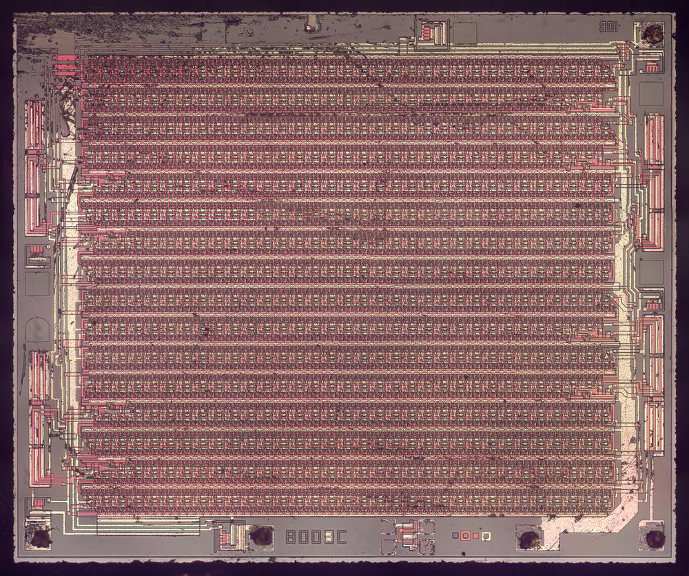
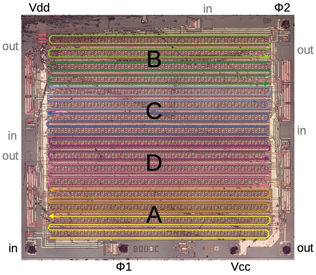
Die of the Signetics 2504 shift register chip. Click this image (or any other) for a larger version.

Die of the Signetics 2504 shift register chip. Click this image (or any other) for a larger version.

The photo above shows the chip under the microscope. The underlying silicon is grayish, with white metal wiring on top. The thickest metal wiring provides power to the chip. The chip also has wiring and transistors constructed from a type of silicon called polysilicon; the polysilicon appears red in the photo. Most of the die is occupied by the shift register, arranged in rows that snake back and forth. The squares around the edge of the die are bond pads, where bond wires connect the die to the chip's external pins.3

The Apple-1's display

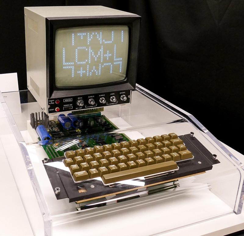
The Apple-1 displayed 24 lines of forty characters on a television monitor. Like most computers at the time, the Apple-1 stored characters rather than pixels to reduce memory requirements. A character-generation ROM converted each character into a 5×7 matrix of pixels as it was displayed. To reduce memory even more, the display didn't store full bytes, but 6-bit characters, supporting upper-case letters, numbers, and some symbols.

The Apple-1 computer was sold as a circuit board. The user had to supply a keyboard, power supply, display, and case. Photo by Cynde Moya, CC BY-SA 4.0.

The Apple-1 computer was sold as a circuit board. The user had to supply a keyboard, power supply, display, and case. Photo by Cynde Moya, CC BY-SA 4.0.

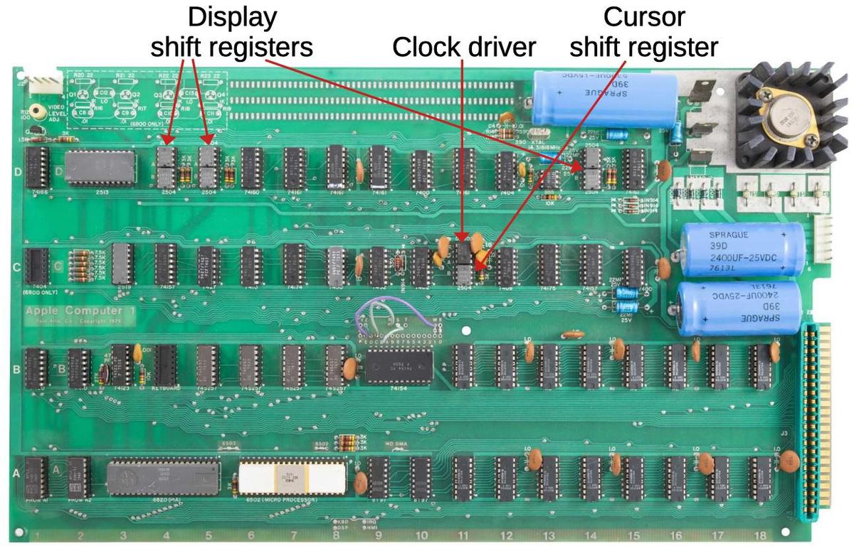
The six-bit display characters were held in six 1024-bit shift registers. A seventh shift register tracked the cursor position.4 The diagram below shows the shift registers and the clock driver on the Apple-1 circuit board. These chips are in 8-pin packages, so two chips fit into the space of a regular TTL chip.5

Apple-1 circuit board, showing the 1024-bit shift register chips and the clock driver chip.
Original image from
Achim Baqué, CC BY-SA 4.0.

Apple-1 circuit board, showing the 1024-bit shift register chips and the clock driver chip. Original image from Achim Baqué, CC BY-SA 4.0.

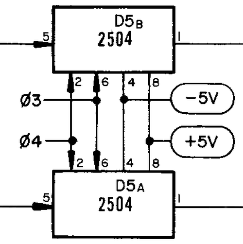
The image below shows how the 2504 shift register chips are represented on the Apple-1 schematic. The chips use just 6 pins. Each chip has a single connection for bits coming in and a connection for the bits coming out. The remaining pins provide the two clock signals and the ±5 volt power supplies. Unlike RAM chips, these chips do not take an address.

Detail of the Apple-1 schematic showing two of the shift register chips.

Detail of the Apple-1 schematic showing two of the shift register chips.

PMOS integrated circuits

This shift register chip was created around 1970, an interesting time in the development of MOS integrated circuits. Early integrated circuits used a type of transistor known as bipolar. However, the metal-oxide-semiconductor (MOS) transistor had the potential to make cheaper, high-density integrated circuits. The first commercial MOS integrated circuit was a 20-bit shift register, created in 1964 by a company called General Microelectronics.

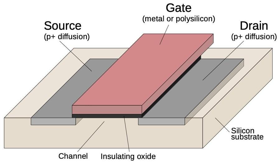
The diagram below shows the structure of a MOS transistor. At the bottom is the silicon, which is doped with impurities to form p-type silicon. The two conductive p-type regions are called the transistor's source and drain. The channel acts as a switch between the source and drain, turned on by voltage in the metal gate above. A thin insulating oxide layer separates the metal gate from the underlying silicon. These three layers—metal, oxide, semiconductor— give the MOS transistor its name. In the late 1960s, chips started to use gates made of polysilicon, a special type of silicon that produced better transistors than metal gates. This is the technology used by the 2504 shift register: the "P-MOS silicon gate process".

Structure of a P-type MOSFET.

Structure of a P-type MOSFET.

By the mid-1970s, however, integrated circuits changed in two more ways. First, P-MOS transistors were replaced by N-MOS transistors, which had better performance. Second, the introduction of ion implantation machines allowed transistor characteristics to be adjusted, with "depletion-mode" transistors8 leading to faster, lower-power circuitry. These changes ushered in the age of popular microprocessors such as the Zilog Z80, MOS Technology 6502, and Intel 8085. These had much better performance than earlier PMOS processors such as the Intel 8008.7 The 6502, of course, was the processor in the Apple-1 (and Apple II).

The shift register

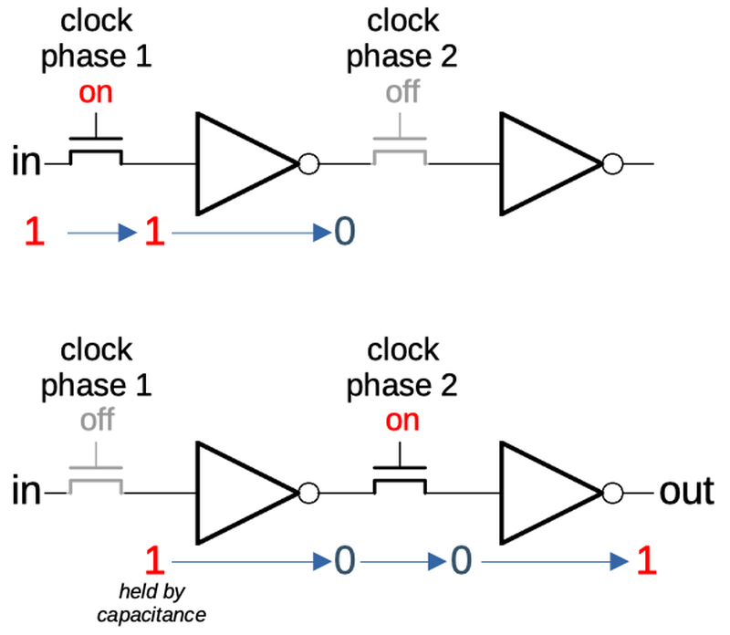
Next, I'll look at the details of how the shift register was constructed. The idea of a shift register is that bits are passed from stage to stage, controlled by clock pulses. With 1024 stages, the shift register can hold 1024 bits. Each shift register stage uses two transistors and two inverters as shown below. During the first clock phase, the first transistor turns on, allowing the input bit to pass through it and the first inverter. During the second clock phase, the second transistor turns on, allowing the inverted value to pass through it and the second inverter, producing the output. Thus, a bit takes two clock phases to move through the shift register stage.

In the first clock phase, the input passes through the first transistor. In the second clock phase, the input is held by the gate capacitance and passes to the output.

In the first clock phase, the input passes through the first transistor. In the second clock phase, the input is held by the gate capacitance and passes to the output.

This circuit is a dynamic shift register, which works due to the circuit's capacitance. When the first transistor turns off, the value remains at the input to the first inverter, held by the capacitance of the circuit. (And likewise for the second transistor.) Because the gate of a MOSFET uses almost no current, the bit value will remain for a couple of milliseconds or so before it drains away. (This is the same principle used by DRAM, holding bits through capacitance.) As long as the clock keeps going, the bit gets refreshed by each stage.

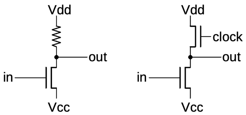
Each inverter is implemented using two MOS transistors. The concept is shown on the left, below. A high input turns on the transistor, which pulls the output low. A low input turns off the transistor allowing the pull-up resistor to pull the output high. Thus, the circuit inverts its input.

Conceptually, the inverter uses the circuit on the left. The implementation uses the circuit on the right.

Conceptually, the inverter uses the circuit on the left. The implementation uses the circuit on the right.

The circuit is actually implemented with a transistor in place of the resistor, as shown on the right, because transistors are more compact than resistors. A high input to the upper transistor turns it on, causing the pull-up current to flow. In a standard inverter, the transistor would be connected to be always on.9 However, the output of the inverter is only used during one clock phase. To reduce power consumption, the transistor is wired to the clock so it only acts as a pull-up when needed.

A shift-register stage on the die

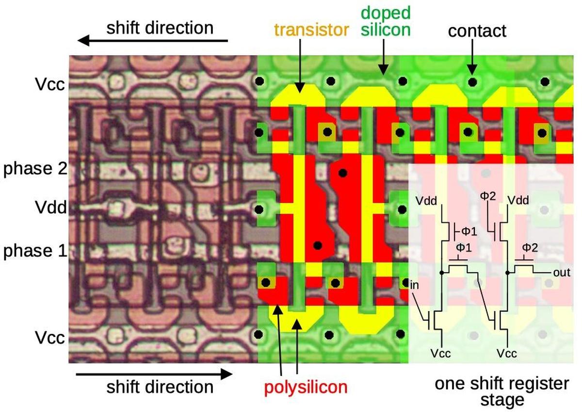
The diagram below shows how shift-register stages are physically constructed on the die. The first part of the image shows how the circuitry appears under the microscope, a complicated jumble of silicon, polysilicon, and metal circuitry. In the middle, I've highlighted the doped silicon in green and the polysilicon in red. A transistor gate (yellow) is formed where polysilicon crosses silicon, with the source and drain on either side. (The horizontal metal wiring should be clear without highlighting.) Note the complex, optimized shapes of the polysilicon and the transistors. Finally, a black dot indicates a contact that connects two layers. In the bottom half of the image, bits are shifted to the right, while in the top half, bits are shifted to the left.

One stage of the shift register.

One stage of the shift register.

In the lower right, one stage of the shift register is represented by a schematic on top of the underlying circuitry. The stage is implemented with six transistors as described earlier. Note that the pull-up transistors to Vdd are long and skinny, reducing their current. The inverter transistors to Vcc, on the other hand, are wide, so they provide a lot of current. The circuitry in the top half of the image is the same, but rotated 180°. Note that the two rows of shift registers share the clock phase lines and Vdd, making the layout more efficient.6

Topology of the chip

You might expect the chip to consist of 1024 shift-register stages arranged into a chain. However, the chip had an unusual topology that allowed it to operate at double speed: one bit per clock phase instead of one bit per complete clock cycle. It accomplished this with a simple trick: it was really two 512-bit shift registers operating in parallel. The first operated on clock phase 1, phase 2, phase 1, ..., while the second was the opposite: phase 2, phase 1, phase 2, ... The result was that one half would produce bits in phase 1, while the other would produce bits in phase 2. The output circuit merged these together into a single output stream. From the outside, it looked like a 1024-bit shift register that operated twice as fast.

Another complication is that Signetics produced three 1024-bit shift register chips from the same silicon layout: the 2502 (organized as four 256-bit shift registers), the 2503 (512×2), and the Apple-1's 2504 (1024×1). The different chips were created by changing the metal wiring of the chip during manufacturing, which was much easier than building completely different chips. To support this, the shift register was broken into eight 128-bit segments, shown below. In the 1024×1 chip, two chains of four 128-bit segments ran in parallel (on opposite clock phases) to produce a 1024-bit shift register. The first chain used the light-colored segments A, B, C, D, while the second chain used the dark-colored segments. The segments are connected by the metal wiring along the side of the die. The chip's pads around the edges are labeled; the grayed-out ones are not used in this chip. The large block of circuitry above the output pin combines the two chains into one output.

The chip consists of 8 shift-register chains, each 128 bits long. They are connected in different ways to form different shift register chips.

The chip consists of 8 shift-register chains, each 128 bits long. They are connected in different ways to form different shift register chips.

The other variants of the chip wire the shift-register segments differently and use additional input and output pins. The 512×2 2503 chip used four chains of 256 bits along with two input and output circuits. The 2502B chip used all eight 128-bit chains in parallel to form a 256×4 shift register, with four input and output circuits.10

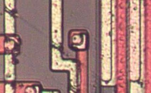
The image below shows one of the unconnected outputs: the red polysilicon wire isn't connected at one end. With a small change to the metal layer, the metal wiring between two segments can be broken and the segment wired to this output instead. The other changes between chip versions are similar.

The polysilicon wire in the middle is disconnected.

The polysilicon wire in the middle is disconnected.

The clock driver

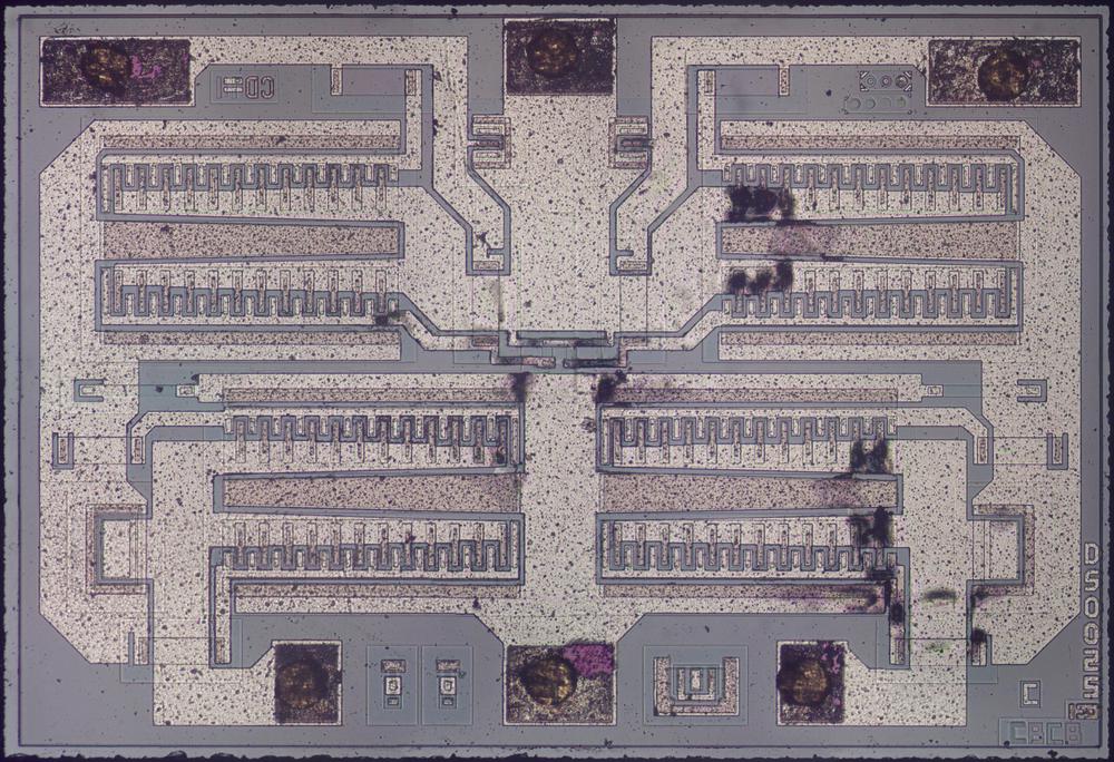
I'll wrap up with a brief mention of the clock driver chip that drives the shift registers. Shift-register memory chips required clock pulses with high current and unusual voltages due to the PMOS circuitry: from +5 volts to -11 volts. These pulses were provided by a special chip, the DS0025 Two-Phase MOS Clock Driver. The die photo below shows this chip. The die is dominated by four power transistors that produced 1.5 amp pulses. I wrote a blog post about the clock driver chip if you want more details.

Die photo of the DS0025 clock driver chip.

Die photo of the DS0025 clock driver chip.

Conclusion

The Apple-1 is now a collector's item, with boards selling for hundreds of thousands of dollars. However, when it was introduced in 1976, it wasn't a particularly important computer, with about 200 sold at the price of $666.66. The Apple II, which came out a year later in 1977, was a much more influential computer, selling millions to become one of the archetypical home computers of that era. The Apple II used RAM chips for all its storage, illustrating that shift-register memory had rapidly become obsolete.

The shift-register chip illustrates the amazing decline in memory prices, as reflected by Moore's Law. This 1-kilobit shift register cost about $60 (in current dollars), while a 16-gigabit DRAM chip now costs about $6. Thus, memory is about 160 million times cheaper now, an amazing drop.

I announce my latest blog posts on Twitter, so follow me @kenshirriff. I also have an RSS feed. Thanks to @TubeTimeUS for supplying the chip. I've written about the Intel 1405 shift register memory if you want to know more about this type of storage.

Notes and references

  1. The first reference to the Signetics 2504 that I could find was in 1970, when each chip cost $11.05 in quantities of 100 (about $60 in current dollars). Looking in an old Byte magazine from 1976, a 1-kilobit shift register chip cost $9 ($34 in current dollars), while a 4-kilobit DRAM chip cost $20 ($75 in current dollars). Thus, it appears that even by the time the Apple-1 was released, DRAMs had become cheaper than shift registers.

    The Apple-1 used 4-kilobit RAM for data and program storage. It's possible, though, to build a computer that uses shift-register storage for its main memory. The Datapoint 2200 is one example. If memory is accessed sequentially, shift-register storage is efficient since the bits are provided sequentially. However, if you access memory out of sequence, the processor has to wait while the memory cycles around, until the desired bits become available. In a way, shift-register memory is a throwback to very early computers such as EDSAC (1949), which used mercury delay lines for main storage. 

  2. The behavior of shift-register memory was a good match for video circuitry, since characters are displayed on the screen in a fixed, repeating order (left to right and top to bottom). The IBM 2260 video display terminal (1965) used a technique similar to shift registers: it stored data in a sonic delay line, sending torsional pulses through a 50-foot nickel wire. But unlike the Apple-1, this delay line stored pixels, not characters. For more about this system, see my blog post

  3. The die was encased in an epoxy package. To expose the die, Eric (@TubeTimeUS) tediously sanded through the plastic package until the die was visible. There are a few scratches on the die from this process, especially in the upper left. 

  4. The display circuitry has some additional complexity. Characters can't be taken directly from the display shift register: since each character is made up of eight scan lines; a line of character must be processed eight times. To handle this, a second shift register (six 40-bit registers) buffers a line of characters and feeds each character into a display ROM. Another 1024-bit shift register keeps track of the cursor position. For more details, see stackexchange

  5. The Apple-1 display has a lot of similarity with the popular TV Typewriter, a hobbyist video terminal kit from 1973. The TV Typewriter used shift-register memory for its 32×16 display, but had a complex 5-board design. Wozniak's design for the Apple-1 was much simpler. 

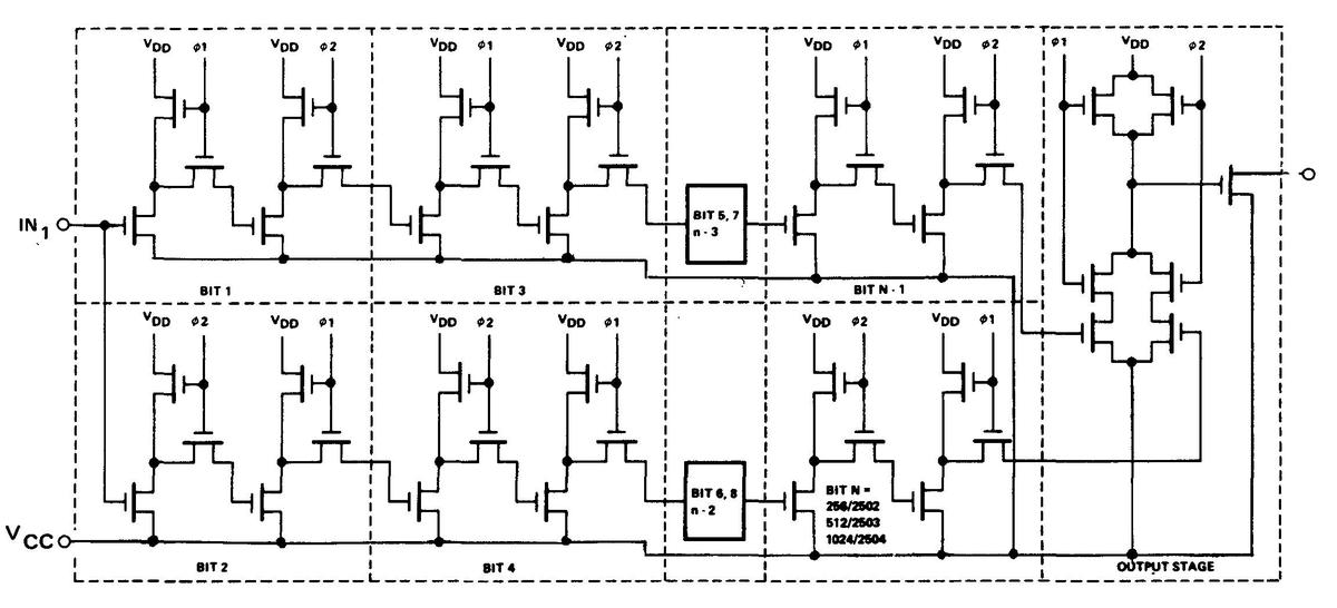
  6. The schematic of the chip is shown below. Notice the upper and lower shift registers, which run on opposite clock phases. Apart from the 6-transistor shift-register stages, the only circuitry is the output stage that merges the two results and drives the output pin.

    Schematic of the chip. Click for a larger image. From the 1972 databook.

    Schematic of the chip. Click for a larger image. From the 1972 databook.


  7. Another major improvement in integrated circuits was the introduction of CMOS, which used NMOS and PMOS transistors together, with much lower power consumption. By the 1980s, processors such as the Intel 80386 (1985) and Motorola 68030 (1987) used CMOS. CMOS is still used in modern integrated circuits. 

  8. In the mid-1970s, ion implantation technology allowed the creation of depletion-mode transistors. These transistors could be used as pull-up elements, called depletion loads. Since depletion-load transistors could operate faster and with less current, they rapidly became a standard part of MOS integrated circuits, until replaced by CMOS in the 1980s. The Zilog Z80 and Intel 2102 SRAM were two early chips that used depletion loads. 

  9. You might think that the inverter circuit will result in a short circuit between Vdd and Vcc when both the input and the clock are high. However, the pull-up transistor is designed to produce a weak current, so the other transistor can still pull the output low. This current results in relatively high power consumption for PMOS or NMOS circuitry, a problem that is fixed by CMOS. 

  10. The 256×4 2502B chip required a 16-pin package, rather than the 8-pin package of other chips, due to the additional input and output pins. 

Inside the Apple-1's unusual MOS clock driver chip

Apple's first product was the Apple-1 computer, introduced in 1976. This early microcomputer used an unusual type of storage for its display: shift register memory. Instead of storing data in RAM (random-access memory), it was stored in a 1024-position shift register. You put a bit into the shift register and 1024 clock cycles later, the bit pops out the other end. Since a shift-register memory didn't require addressing circuitry, it could be manufactured more cheaply than a random-access memory chip.1 The downside, of course, is that you had to use bits as they became available, rather than access arbitrary memory locations. The behavior of shift-register memory was a good match for video circuitry, though, since characters are displayed on the screen in a fixed, repeating order (left to right and top to bottom).2


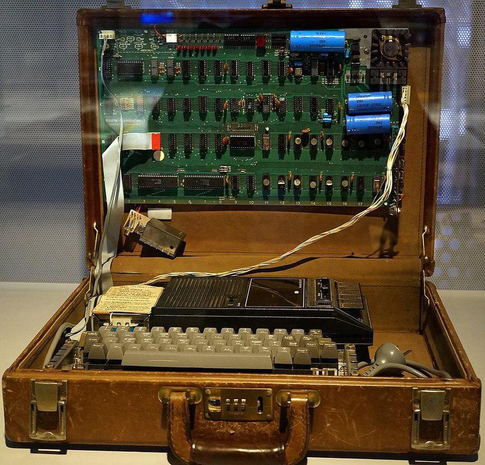
The Apple-1 was sold as a bare board, so users needed to make a case for it, or mount it in a briefcase as shown here.
Note the cassette drive used for mass storage.
Photo cropped from Binarysequence, CC BY-SA 4.0.

The Apple-1 was sold as a bare board, so users needed to make a case for it, or mount it in a briefcase as shown here. Note the cassette drive used for mass storage. Photo cropped from Binarysequence, CC BY-SA 4.0.

Shift-register memory chips required clock pulses with high current and unusual voltages: from +5 volts to -11 volts. These pulses were provided by a special chip, the DS0025 Two-Phase MOS Clock Driver. This chip, introduced in 1969, was the first monolithic (i.e. integrated circuit) clock driver. In this blog post, I look inside the chip and explain how it was implemented.

Die of the DS0025 clock driver. Click this image (or any other) for a larger version.

Die of the DS0025 clock driver. Click this image (or any other) for a larger version.

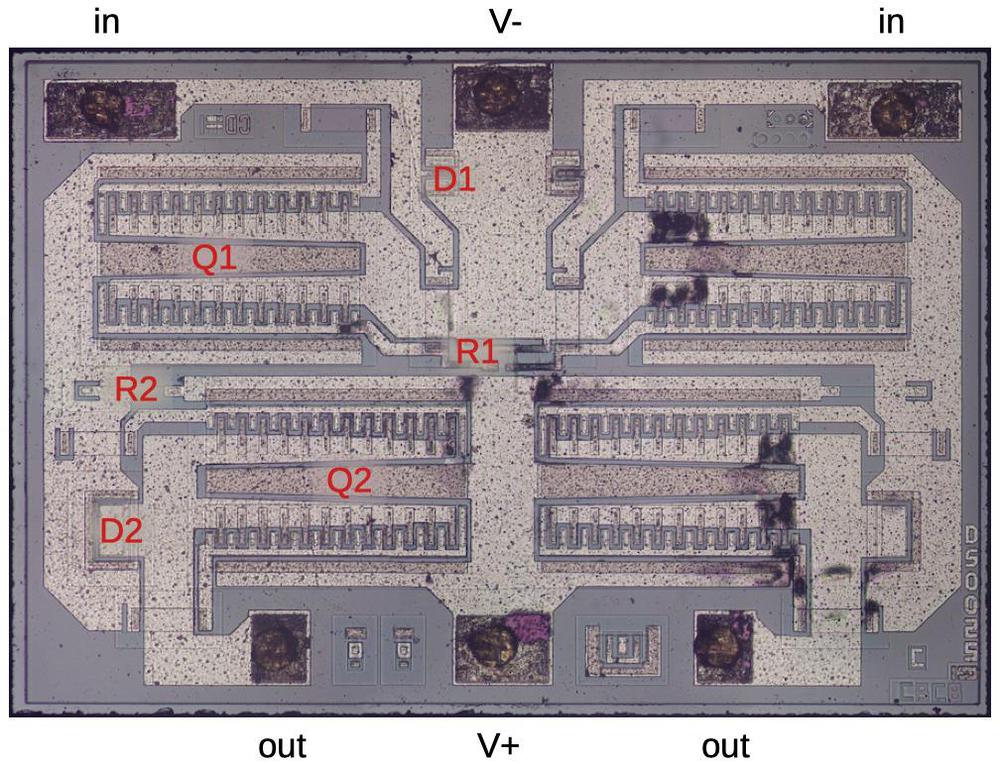
The photo above shows the silicon die under the microscope. This chip is very simple, containing four large NPN transistors, four diodes, and four resistors. The silicon appears blue-gray in this image, while the metal layer on top appears speckled white. Around the outside of the die, are six dark rectangles, the pads where golden bond wires connected the die to the chip's external pins.

The die was encased in an epoxy package. To expose the die, Eric (@TubeTimeUS) tediously sanded through the plastic package until the die was visible. Some bits of epoxy remained, caught in the bond wires, so I cleaned up the die with a few drops of boiling sulfuric acid.

The Apple-1's display

The Apple-1 displayed 24 lines of forty characters on a television monitor. Like most computers at the time, the Apple-1 stored characters rather than pixels to reduce memory requirements. A character-generation ROM converted each character into a 5×7 matrix of pixels as it was displayed. To reduce memory even more, the display didn't store full bytes, but 6-bit characters, supporting upper-case letters, numbers, and some symbols.

The six-bit display characters were held in six 1024-bit shift registers. A seventh shift register tracked the cursor position.3 The diagram below shows the shift registers and the clock driver on the Apple-1 circuit board. These chips are in 8-pin packages, so two chips fit into the space of a regular TTL chip.

Apple-1 circuit board, showing the 1024-bit shift register chips and the clock driver chip.
Original image from
Achim Baqué, CC BY-SA 4.0.

Apple-1 circuit board, showing the 1024-bit shift register chips and the clock driver chip. Original image from Achim Baqué, CC BY-SA 4.0.

Transistors

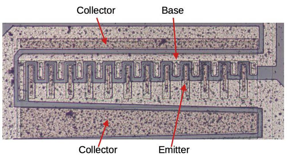
Next, I'll discuss the components of the chip. Because the chip generates high-current pulses, it uses large NPN transistors, with a different construction from most integrated circuit transistors. Each transistor consists of 24 emitters, paralleled in two groups. (You can consider it one large transistor, 2 transistors, or 24 small transistors.) The transistor is structured vertically with the collector (made of N-doped silicon) underneath, a thin P-type base in between, and the N-type emitters embedded in the top, forming the N-P-N layers of the transistor. The doped silicon regions are faintly visible with black lines around their boundaries.

Half of a transistor, with 12 emitters.

Half of a transistor, with 12 emitters.

In the photo above, you can see the metal wiring for the transistor's collector, base, and emitter. The collector wiring is on the outside, with base wiring in between. The collector and emitter wiring is tapered: at one end, the wiring needs to support the full current load, while at the other end it only handles 1/12 of the current. The tapered approach saves space, since it is thicker only where it needs to be thick.

Resistors

The resistors are formed from silicon doped to have higher resistance. The doped silicon rectangle is faintly visible in the die photo. At each end of the resistor, a contact connects the silicon to the metal layer on top. The 1000Ω resistor on the left is longer than the 250Ω resistor on the right, giving it more resistance.

Two resistors as they appear on the die.

Two resistors as they appear on the die.

"Tunnels"

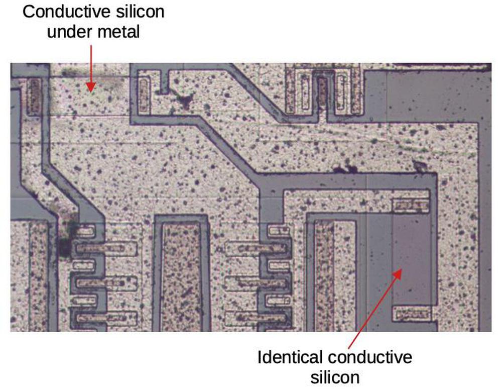
The chip has a single layer of metal wiring, which poses a problem if two signals need to cross. The solution is to put one signal in the silicon layer so it can pass under the metal layer. In essence, a low-valued resistor is used to pass under the metal layer. The image below shows how a tunnel appears on the die.

The conductive silicon strip at the top connects the metal regions on either side. The conductive strip at the bottom doesn't fulfill a wiring need, but ensures that both paths encounter the same resistance.

The conductive silicon strip at the top connects the metal regions on either side. The conductive strip at the bottom doesn't fulfill a wiring need, but ensures that both paths encounter the same resistance.

One problem is that the silicon has relatively high resistance compared to metal, so the tunnel adds resistance. The chip is carefully designed so both "sub-transistors" encounter the same resistance, to avoid one transistor turning on before the other. You can see that the input path in the upper left has a tunnel to pass under the metal wiring, while the path in the lower right has a tunnel of identical dimensions that doesn't go under any metal. While the second tunnel appears pointless, it assures that both paths have the same resistance.

The chip's circuit

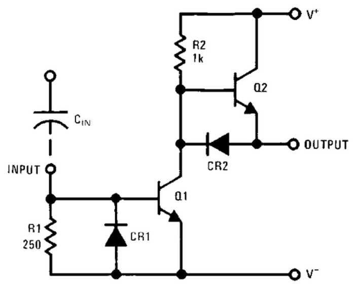
The shift register requires a two-phase clock, that is two clock signals in alternation that step the bits through the circuit. To support this, the clock driver chip has two identical driver circuits. The schematic below shows one of the circuits. When the input goes high, it turns on transistor Q1, pulling its collector low. This pulls the output low through diode CR2. When the input drops, Q1 turns off. This lets R2 provide a current to the base of Q2, turning it on, and pulling the output high. Thus, the circuit is essentially an inverter, but one that can provide up to 1.5 amps of output.4

Schematic of the DS0025, from the application note.

Schematic of the DS0025, from the application note.

The image below shows the various components of the schematic as they appear on the die. Most of the chip is occupied by the large power transistors. Although the chip is mounted in an 8-pin package, only six pins are used; the corresponding pads are labeled below. The chip consists of two identical mirror-image drivers; one is labeled. There are a few blackened regions in the transistors; we suspect this is where the chip failed.

Die with the components labeled.

Die with the components labeled. Note: diodes are labeled CR (crystal rectifier) in the schematic but D here.

Conclusion

This chip provides an interesting view of computer technology in the 1970s. The Apple-1 used shift-register memory, a technology that rapidly became obsolete as RAM prices dropped. Shift-register memory required a specialized clock driver integrated circuit, a chip that contained just four large transistors. With billions of transistors in modern integrated circuits, it's hard to imagine that it was once worthwhile to build a chip that was this simple. The Apple II, introduced just a year later in 1977, used RAM chips for all its storage, making shift-register memory a thing of the past.

I announce my latest blog posts on Twitter, so follow me @kenshirriff. I also have an RSS feed. Thanks to @TubeTimeUS for supplying the chip. I've written about the Intel 1405 shift register memory if you want to know more about this type of storage.

Notes and references

  1. Looking in an old Byte magazine from 1976, a 1-kilobit shift register chip cost $9 ($34 in current dollars), while a 4-kilobit DRAM chip cost $20 ($75 in current dollars). Thus, it appears that even by the time the Apple-1 was released, DRAMs had become cheaper than shift registers. (This also illustrates the amazing drop in memory prices since the 1970s, as described by Moore's Law.)

    The Apple-1 used 4-kilobit RAM for data and program storage. It's possible, though, to build a computer that uses shift-register storage for its main memory. The Datapoint 2200 is one example. If memory is accessed sequentially, shift-register storage is efficient since the bits are provided sequentially. However, if you access memory out of sequence, the processor has to wait while the memory cycles around, until the desired bits become available. In a way, shift-register memory is a throwback to very early computers such as EDSAC(1949), which used mercury delay lines for main storage. 

  2. The IBM 2260 video display terminal (1965) used a technique similar to shift registers: it stored data in a sonic delay line, sending torsional pulses through a 50-foot nickel wire. But unlike the Apple-1, this delay line stored pixels, not characters. For more about this system, see my blog post

  3. The display circuitry has some additional complexity. Characters can't be taken directly from the display shift register: since each character is made up of eight scan lines; a line of character must be processed eight times. To handle this, a second shift register (six 40-bit registers) buffers a line of characters and feeds each character into a display ROM. Another 1024-bit shift register keeps track of the cursor position. For more details, see this post. The Apple-1 schematic is in the Operation Manual

  4. The large current is required because of the design of the shift-register memory. The clock line snakes through the chip, providing a clock signal to each stage of the shift register. As a result, the clock line has a fairly high capacitance, about 150 picofarads. This clock line must be switched between +5 volts and -11 volts at a 1 megahertz rate. The combination of large capacitance and large voltage swing with the fast rate requires a high current. 

Inside the stacked RAM modules used in the Apple III

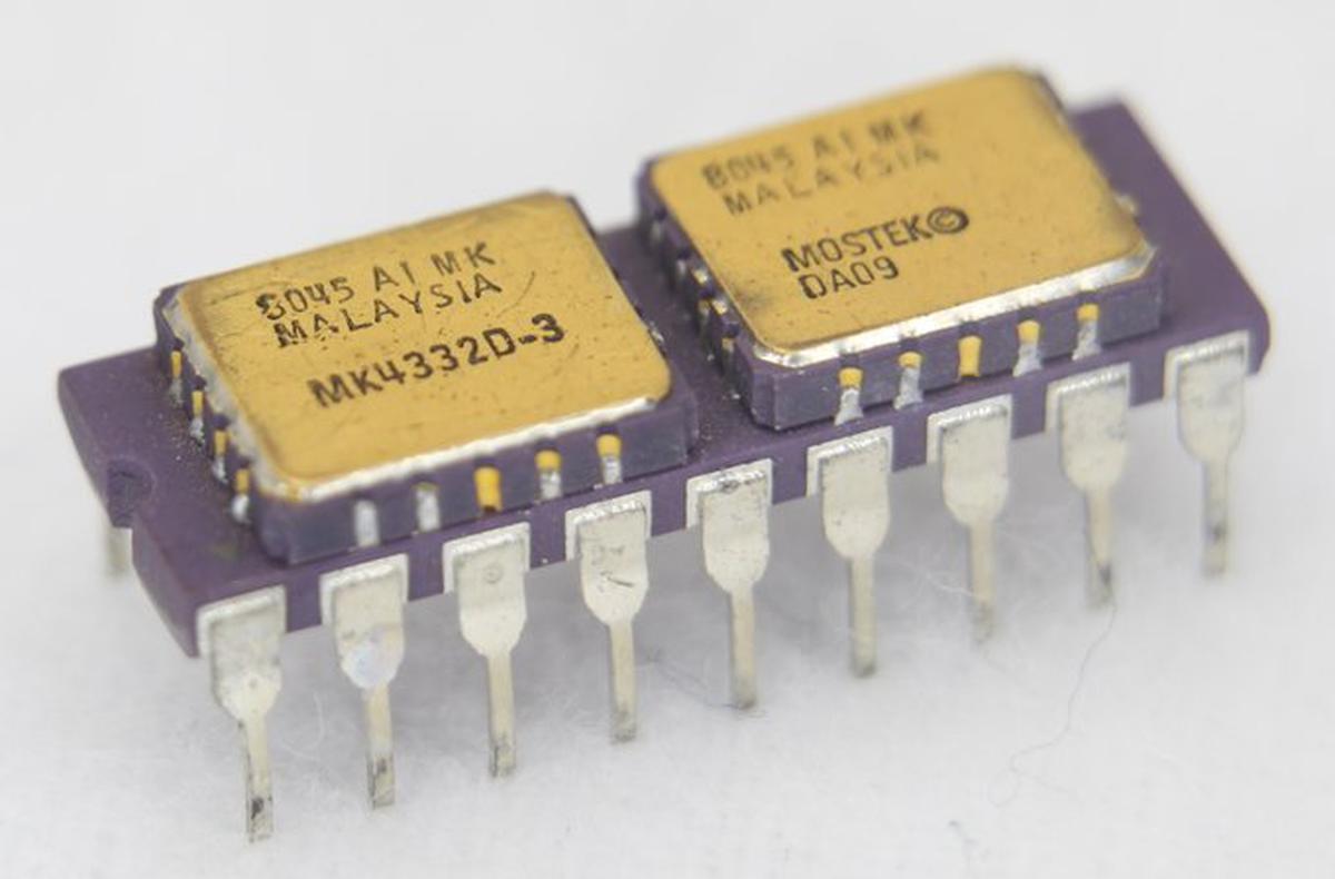
In 1978, a memory chip stored just 16 kilobits of data. To make a 32-kilobit memory chip, Mostek came up with the idea of putting two 16K chips onto a carrier the size of a standard integrated circuit, creating the first memory module, the MK4332 "RAM-pak". This module allowed computer manufacturers to double the density of their memory systems and by 1982, Mostek had sold over 3 million modules. The Apple III is the best-known system that used these memory modules.

The MK4332 memory module combined two 16-kilobit memory chips on a ceramic substrate.

The MK4332 memory module combined two 16-kilobit memory chips on a ceramic substrate.

This module was built from two 16-kilobit memory chips, constructed from the standard MK4116 dynamic RAM (DRAM) chip packaged in a leadless ceramic chip carrier; these are the golden rectangles on top of the carrier.

You might wonder why customers didn't simply use these surface-mount packages directly, but at the time soldering surface-mount components was still a challenge for many customers. However, mounting two leadless chips on a dual inline-package (DIP) carrier allowed customers to double their memory density while still using their standard through-hole soldering techniques.

The purple carrier holding the chips was a ceramic substrate designed for thermal compatibility with the chips.1 There is no circuitry inside the ceramic carrier except wiring between the chips and the eighteen DIP pins. The two memory chips were wired in parallel except for their two select lines, which were kept separate. This allowed the desired memory chip to be selected. As a result, the MK4332 module has 18 pins, compared to 16 pins for the chips on top. Mostek used the same module design with the next generation of RAM chips, creating a 128-kilobit RAM module (MK4528) from two 64-kilobit RAM chips (MK4564).

Inside the 4116 memory chip

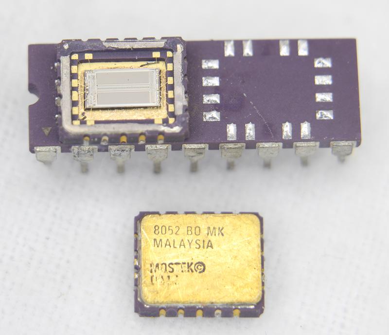
Although you might expect a complex mounting technique, the two 4116 chips are simply soldered onto the substrate with standard reflow techniques. For the photo below, I removed the metal lid from the left chip with a chisel and unsoldered the right chip with a hot air gun. On the left, you can see the rectangular silicon die inside the leadless carrier package. On the right are the 16 solder pads on the ceramic substrate. The wiring between the solder pads and the DIP pins is inside the ceramic substrate.

The MK4332 with the left package opened and the right package unsoldered.

The MK4332 with the left package opened and the right package unsoldered.

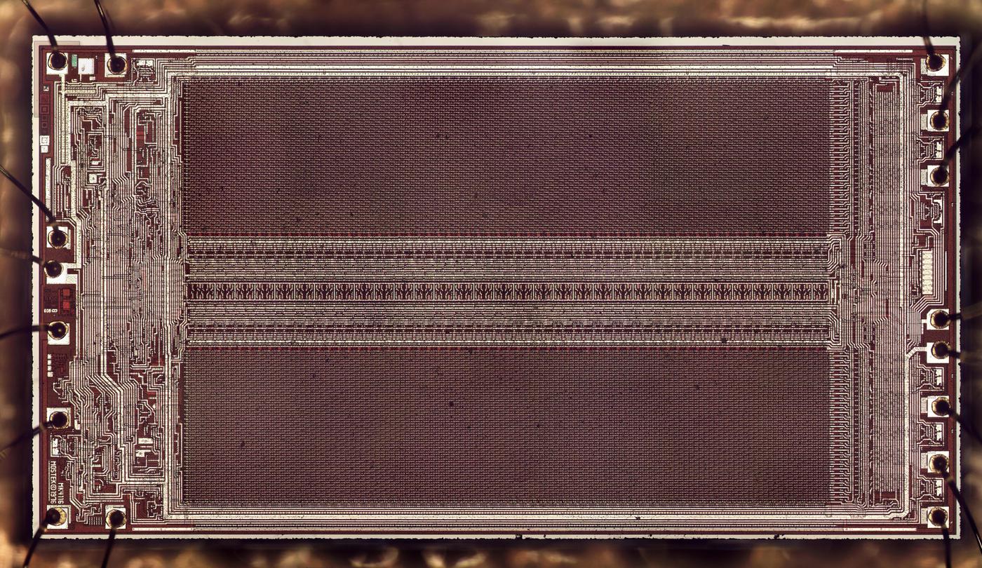
I created the die photo below from multiple microscope images. The white lines are the metal wiring on top of the chip, while the silicon underneath appears dark red. The two large rectangular regions are the 16,384 memory cells, arranged as a 128×128 matrix, split in two. The circuitry in between these regions consists of 128 sense amplifiers to amplify the bits read from memory, and selection circuitry to select one bit out of the 128. (Externally, the chip is accessed as 16,384×1, outputting a single bit. Typically, eight of these chips were used to store bytes.) The control and interface circuitry is at the left and right, connected to the external pads via tiny bond wires.

Die photo of the 4116 memory chip. Click for a larger image.

Die photo of the 4116 memory chip. Click for a larger image.

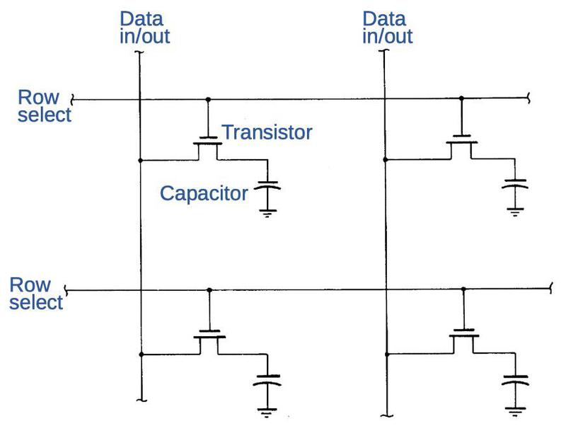
In dynamic RAM, a bit is stored in a capacitor, with a transistor providing access to the capacitor. The value of the bit is represented by the presence or absence of charge on the capacitor. The advantage of dynamic RAM is that each memory cell is very small, constructed from just two components,2 allowing a high memory density. (In comparison, static RAM may require six transistors per cell.) The downside of dynamic RAM is that the charge on a capacitor leaks away after a few milliseconds. To avoid losing data, dynamic RAM must be constantly refreshed: bits are read from the capacitors, amplified, and then written back to the capacitors. For this particular chip, all the data must be refreshed every two milliseconds.

The diagram below illustrates the wiring of the memory cells, showing two of the 128 rows and columns. To read or write data, a row select line is energized. The transistors in that row turn on, connecting that row's capacitors to the data in/out lines. The data from that row is read out of the capacitors and amplified. At that point, the data can either be written back to refresh the row, or a new bit can be written. Note that although the chip accesses 128 bits in parallel internally, the chip provides access to one bit at a time externally, selecting one of the 128 bits to read or write.

Structure of the memory cells, based on the patent.

Structure of the memory cells, based on the patent.

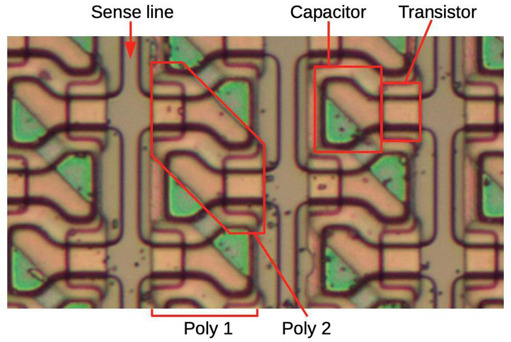
The magnified photo below shows some of the storage cells, densely packed together. It's a bit hard to visualize what's going on because the chip is constructed from multiple layers. The bottom layer is the grayish silicon die. On top of the silicon are two layers of polysilicon. Above this is the metal wiring, which was removed for this photo. The photo shows three sense lines (data in/out) in the silicon, with bulb-shaped storage cells connected on either side. Vertical strips of polysilicon (poly 1) over the storage cells implement capacitors: the silicon forms the lower plate, while the polysilicon forms the upper plate. The second layer of polysilicon (poly 2) is arranged in diagonal regions to implement the selection transistors. Square notches in the poly 1 layer allow the poly 2 layer to approach the silicon to form transistors. Horizontal metal wiring (not visible) is connected to the poly 2 regions to select a row by driving the transistors. Note that the rows are staggered and interlocking (kind of like a zipper) due to the highly-optimized layout. At the time, fitting this much memory on a chip was a challenge that pushed the limits of integrated circuit technology.

A closeup of the memory chip under the microscope, showing individual storage cells.

A closeup of the memory chip under the microscope, showing individual storage cells.

Memory chips in the Apple III

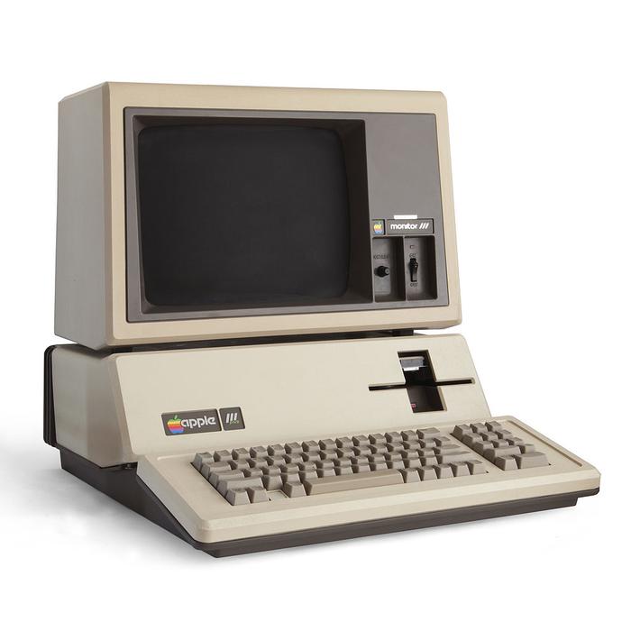
Apple was a major customer of these memory modules, using them in the Apple III computer (1980). The Apple III was marketed as a business computer to follow the popular Apple II. Unfortunately, the Apple III was a business failure due to reliability issues and competition from the IBM PC introduced a year later.

Apple III Plus computer. Photo by Bilby, CC BY 3.0.

Apple III Plus computer. Photo by Bilby, CC BY 3.0.

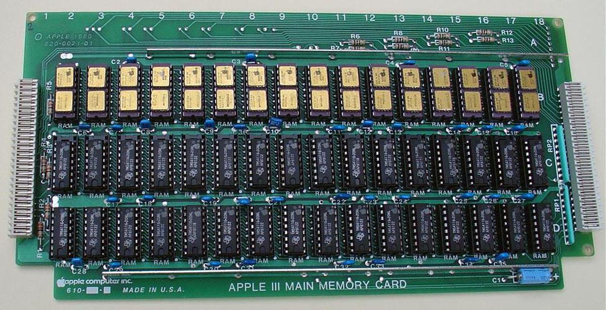
As was usual for the time, the Apple III's memory board3 was stuffed with memory chips to achieve more capacity. An unusual part of the design is it used three rows of memory chips (instead of a power of two), mixing 16-kilobit and 32-kilobit memory chips to achieve 128 kilobytes of storage. (The Apple III's case was designed before the boards, so the boards had to be designed to fit the available space.) In the photo below, the top row holds MK4332 memory modules, while the bottom two rows hold 16-kilobit MK4116 chips.4

Apple III main memory card. Photo courtesy of DigiBarn, CC BY-NC 3.0

Apple III main memory card. Photo courtesy of DigiBarn, CC BY-NC 3.0

A brief history of memory

Memory is an under-appreciated part of computing. The CPU usually gets the attention, but memory was often the limiting factor. The problem with memory is that storing a single bit is easy, but most approaches are impractical when you try to scale up to thousands or millions of bits.

The early ENIAC computer (1946) used vacuum tubes for storage, but these were bulky and expensive, limiting ENIAC to just 20 words (of 10 digits) stored in its accumulators. Early computers such as EDSAC (1949) used mercury delay lines for memory, sending pulse trains of sound waves through tubes of mercury. Although EDSAC could store 512 words, you had to wait for bits to circulate serially through the mercury. An improvement was the random-access Williams tube which stored data as spots on a cathode-ray tube screen. Although they were temperamental, Williams tubes were used in the Manchester Mark 1 (1949) and the commercial IBM 701 (1952).

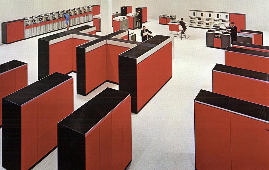
The introduction of core memory revolutionized computing, providing fast, cheap, and reliable storage, storing each bit in a tiny magnetized ferrite ring. Core memory was introduced in the Whirlwind computer (1953) and used in most computers of the late 1950s and 1960s. However, since each bit required a separate physical ferrite core, memory sizes were limited to a few megabytes for even the largest customers. For example, memory cabinets for the IBM System/360 (1969) held 256 kilobytes but weighed over a ton each (below).

Magnetic core memory was relatively bulky. This photo shows an IBM System/360 Model 85 installation. The cabinets in the front are IBM 2365 Processor Storage, each holding 256 kilobytes. The double-H cabinet in the center is the CPU. Photo from IBM.

Magnetic core memory was relatively bulky. This photo shows an IBM System/360 Model 85 installation. The cabinets in the front are IBM 2365 Processor Storage, each holding 256 kilobytes. The double-H cabinet in the center is the CPU. Photo from IBM.

Semiconductor memory led to another dramatic shift. At first, semiconductor memory was costly and had very small capacity; Intel's first product was a memory chip holding just 64 bits and costing $99.50. In 1968, Dennard at IBM invented cost-effective dynamic RAM and semiconductor DRAM technology advanced quickly at various companies. Intel introduced the first commercially available DRAM chip in 1970, the i1103 holding 1K bits. This chip was nicknamed the "core killer" because of its impact on the magnetic core memory industry.

Computer storage rapidly moved from core memory to DRAM as the capacity of DRAM increased and the price fell.5 Mostek introduced the 4-kilobit MK4096 chip in 1973, followed by the 16-kilobit MK4116 in 1976. In 1978, Fujitsu introduced the first commercial 64-kilobit DRAM chip and Japan took the lead in DRAM manufacturing.6 Intel left the DRAM industry in 1985 due to decreasing market share and profits, followed by the remaining US DRAM manufacturers.

Fifty years after the introduction of DRAM, it is still the dominant technology for main storage, a remarkably long lifetime. Compared to the 16-kilobit chip I described, Samsung's recent 16-gigabit DRAMs are a factor of a million larger, showing the incredible increase in density. It remains to be seen if anything will challenge the long storage leadership of DRAM.

I announce my latest blog posts on Twitter, so follow me at kenshirriff. I also have an RSS feed. Thanks to Mike Braden for suggesting the MK4332 chip to me.

Notes and references

  1. For details on the construction of the memory modules, see Rectangular chip-carriers double memory-board density, Electronics, 1982. 

  2. Early dynamic RAMs such as the Intel 1103 used three transistors per cell and used separate lines for reading and writing data. Improvements in memory technology shrunk the circuit to a single transistor and a single data line. 

  3. The Apple III memory board pictured is the "12 volt memory board", given that name because the memory chips required 12 volts (as well as +5 and -5). It was upgraded by the "5 volt memory board", which used only a 5 volt supply. The 5 volt memory board used more modern 64-kilobit memory chips (4864) giving it a larger capacity of 128 or 256 kilobytes. Inconveniently, the power supply required a 12-volt load to operate, so the 5-volt memory board has a power resistor to draw 0.4 amps from the otherwise-unused 12-volt supply. Details are in the Apple III reference manual

  4. The Apple III memory board was also available in a lower-cost 96-kilobyte module. In that configuration, the 4332 memory modules were replaced with the 16-kilobit (MK4116) chips used on the rest of the board. One clever feature of the 4332 module is the two "extra" select pins are on the end of the package. The result is that a memory board (such as the Apple III's) can be designed to accept either the 16-pin 16-kilobyte chips or the 18-pin 32-kilobyte modules, depending on how much memory is desired. With the smaller chips, the two extra pins are unused. It's strange, however, that the Apple III memory board only accepted the larger modules in one of the three rows of chips. 

  5. The industry switch from magnetic core memory to semiconductor memory wasn't as straightforward as superior semiconductor memory overthrowing inferior core memory. Instead, there was a time period where they co-existed, due to tradeoffs. For instance, in 1972, a customer could select core memory, semiconductor memory, or a mixture for the D-112 minicomputer (a PDP-8 clone); semiconductor memory was 5 times faster, but core memory supplied four times the capacity per board. By 1973, industry publications were reporting that "Semiconductor memories are taking over data-storage applications". As late as 1980, core memory manufacturers were advertising the benefits of core memory, battling the "myths" that semiconductor was better.

    Was the overthrow of magnetic core by semiconductor memory inevitable? My view is that "technological determinism" acts in some ways; the development of DRAM memory was almost unavoidable following the development of MOS transistors. However, "economic determinism" was more responsible for the success of semiconductor memory: if magnetic core had remained the lower-cost option, it probably would have remained dominant. As a counterexample, CCD (charge-coupled device) memory and bubble memory were hyped as storage technologies of the future, but couldn't achieve the price-performance to dislodge either semiconductor memory or hard disks. 

  6. Note that the capacity of memory chips increased by a factor of 4 each generation (1-, 4-, 16-, 64-kilobit) rather than a factor of 2. The reason is that each address pin was multiplexed to provide two address bits, so each additional address pin resulted in a factor of four increase. By reusing each address pin for both a row address and a column address, the number of address pins was kept low so compact 16-pin packages could be used even as memory sizes expanded to 256-kilobit. Conveniently, as technology improved, memory chips required fewer voltages, freeing up pins formerly used for power. One consequence, though, was the ordering of address pins on the chip was essentially random as new address pins were assigned based on which pins were available, rather than sequentially. The multiplexed address system was introduced in the Mostek MK4096 chip and meant that the 256-kilobit 41256 chip used fewer pins than the original 1-kilobit Intel 1103 (16 pins vs 18). 

A visit to the Large Scale Systems Museum

I didn't expect to find two floors filled with vintage computers in a small town outside Pittsburgh. But that's the location of the Large Scale System Museum, housed in a former department store. The ground floor of this private collection concentrates on mainframes and minicomputers from the 1970s to 1990s featuring IBM, Cray, and DEC systems, along with less common computers. Amazingly, most of these vintage systems are working. Upstairs, the museum is filled with vintage home computers from the pre-PC era.

IBM

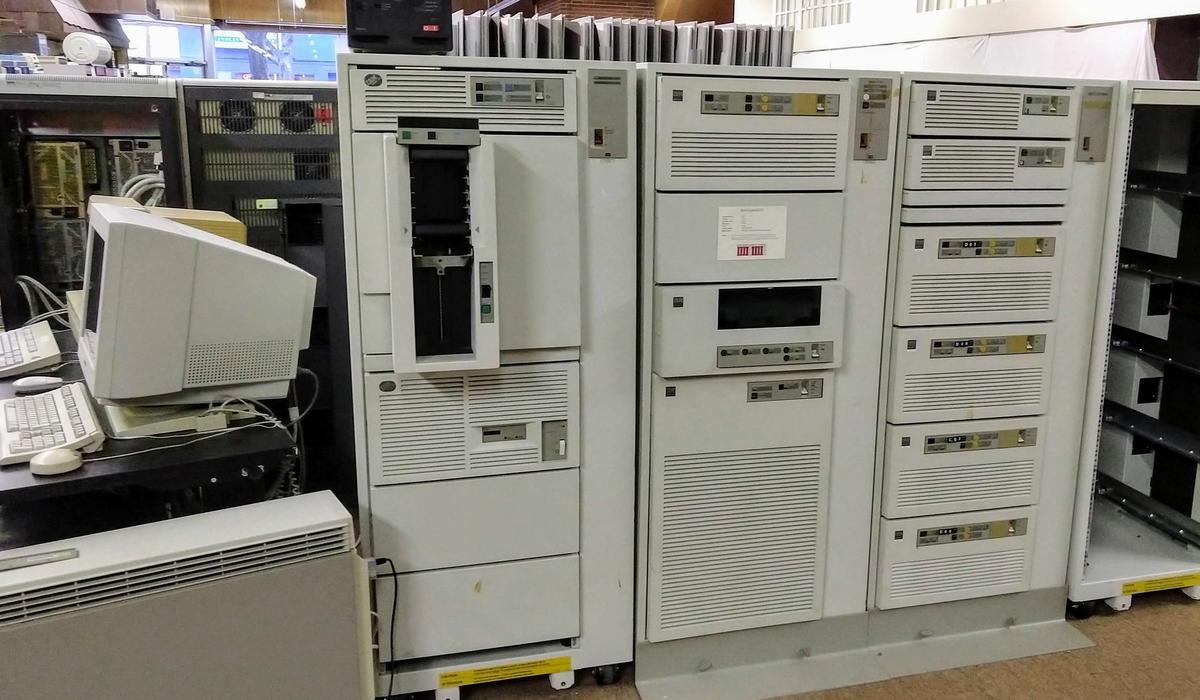
IBM set the standard for the mainframe computer with its introduction of the System/360 in 1964, a line of computers designed to support the full circle (i.e. 360°) of business and scientific applications. The System/360 evolved into the System/370 in the 1970s and the System/390 in the 1990s. Most of these mainframes filled a data center, but the museum has some smaller S/370 and S/390 mainframes designed for offices. The IBM System/370 9375 (1986; below), is described as a "baby mainframe" or "super-mini computer" for engineering or commercial applications.

IBM System/370 9375. The computer itself is in the middle rack. The left rack has a 3490E tape cartridge storage system, while the right rack holds 9335 disk controllers and disk drives (856 MB per drive).

IBM System/370 9375. The computer itself is in the middle rack. The left rack has a 3490E tape cartridge storage system, while the right rack holds 9335 disk controllers and disk drives (856 MB per drive).

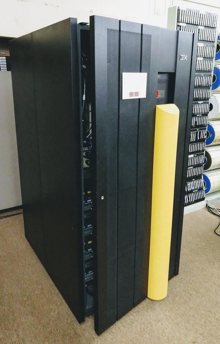
The System/390 line is represented by the IBM System/390 Multiprise-2003 (1997; below). This mainframe could not boot up on its own, but required a special desktop PC called the Mainframe Service Element (photo) to initialize the mainframe with microcode and start it up.

This low-end IBM System/390 Multiprise-2003 had 1 GB of memory and supported hundreds of simultaneous database transactions.

This low-end IBM System/390 Multiprise-2003 had 1 GB of memory and supported hundreds of simultaneous database transactions.

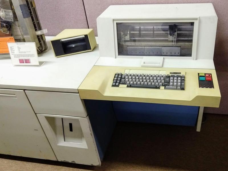
To support smaller customers, IBM also produced minicomputers, which they called "midrange systems". The IBM System/32 (1975; below) is a minicomputer built into a desk, designed for small businesses. IBM's midrange systems evolved into the IBM AS/400 (1992; photo).

This IBM System/32 had 16 KB of memory and 13 MB of disk storage. It leased for $1200 per month.

This IBM System/32 had 16 KB of memory and 13 MB of disk storage. It leased for $1200 per month.

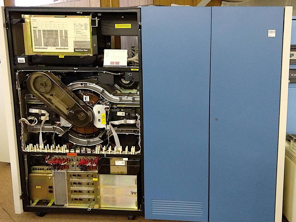
The museum has many disk drives and tape drives. One example is the massive 3380E disk drive (below; 1985), providing 5 gigabytes of storage. It's amazing to think that you can now hold a thousand times as much storage in your hand.

The IBM 3380E disk system stored 5 gigabytes of data. The 14-inch disk platter is in the center, labeled "E".

The IBM 3380E disk system stored 5 gigabytes of data. The 14-inch disk platter is in the center, labeled "E".

Cray

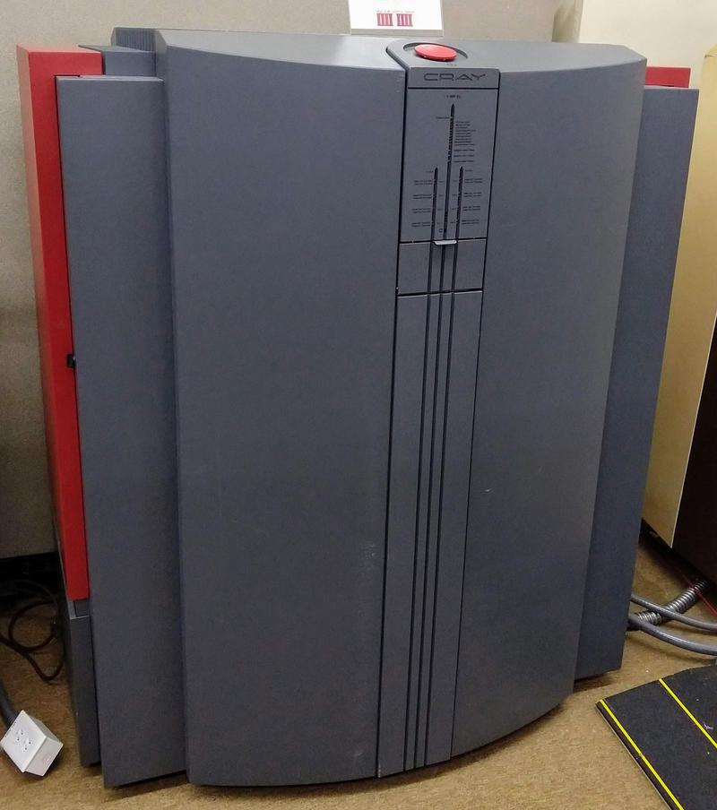
Computer designer Seymour Cray and his company Cray Research were famed for building the world's fastest supercomputers. The museum has several Cray computers from the 1990s. The Cray YMP-EL supercomputer (1992; below) was an "Entry Level" Cray, costing $300,000. It was built from CMOS chips rather than the fast but hot ECL chips in earlier Crays, allowing it to be air-cooled rather than Freon cooled. The museum also has the related, low-end Cray EL-94, packaged in an ugly box (photo; 1992);

The Cray YMP-EL supercomputer.

The Cray YMP-EL supercomputer.

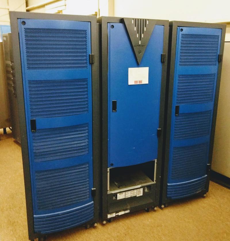
The Cray J90 (1996; below) was a popular low-end Cray, an evolution of the Y-MP EL. This one holds 1 GB of memory and cost $300,000.

Cray J 90 supercomputer.

Cray J 90 supercomputer.

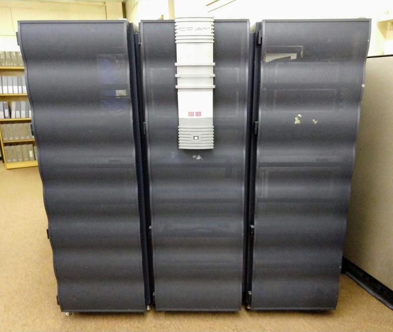
The Cray SV1 (1999; below) followed the J90. It introduced more high-performance features such as a vector cache and multi-streaming. This one has 16 processors and 16 GB of memory, and cost about $1 million.

The Cray SV1 supercomputer.

The Cray SV1 supercomputer.

Digital Equipment Corporation (DEC)

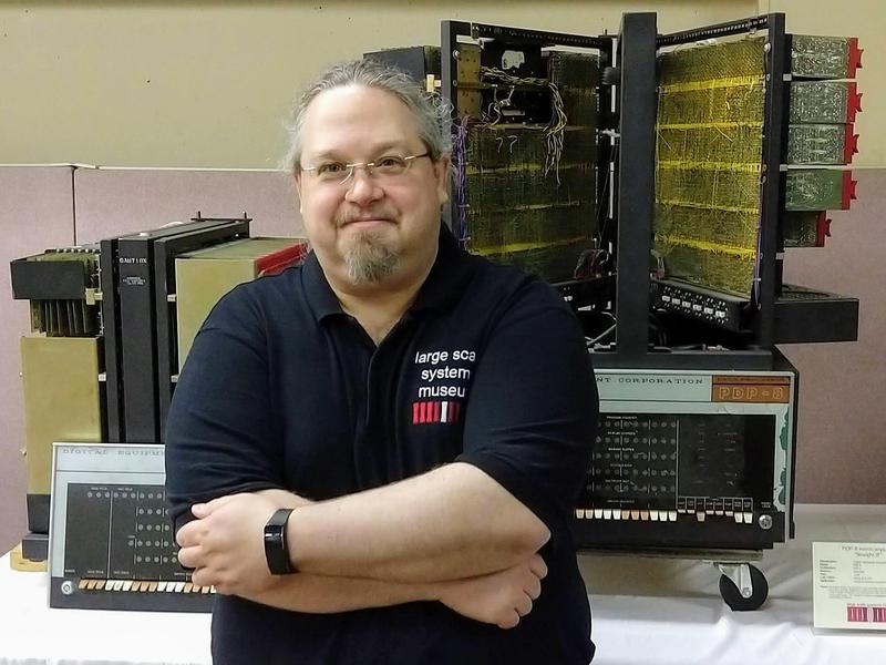
Dave McGuire, curator of the large systems, in front of PDP "Straight 8" minicomputers.

Dave McGuire, curator of the large systems, in front of PDP "Straight 8" minicomputers.

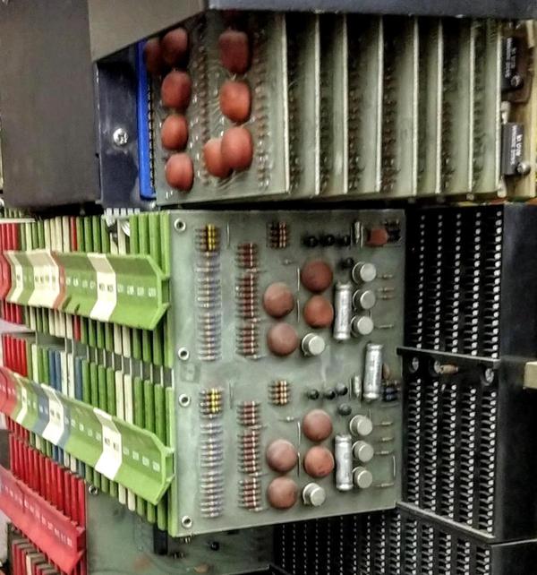
Digital Equipment Corporation was founded in 1957 and became the second-largest computer manufacturer, concentrating on minicomputers. DEC's PDP-8 was a very popular 12-bit minicomputer that essentially created the "minicomputer" category of computers. The first PDP-8 was the Straight-8 (1966; photos above and below), a compact all-transistor computer built from circuit cards plugged into a wire-wrapped backplane.

The "Straight 8" PDP-8 was built from transistorized circuits on small cards.

The "Straight 8" PDP-8 was built from transistorized circuits on small cards.

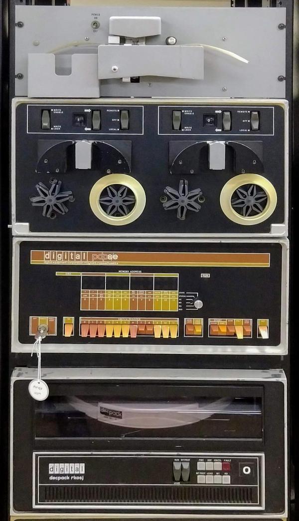
The PDP-8/E (1969; below) used integrated circuits (7400-series TTL) in place of discrete transistors as did the compact and cheaper PDP-8/A (1974; photo).

PDP-8/E minicomputer. The paper tape reader is at the top, above the front panel. An RK05 DECpack is at the bottom, storing 2.4 megabytes on a removable disk pack.

PDP-8/E minicomputer. The paper tape reader is at the top, above the front panel. An RK05 DECpack is at the bottom, storing 2.4 megabytes on a removable disk pack.

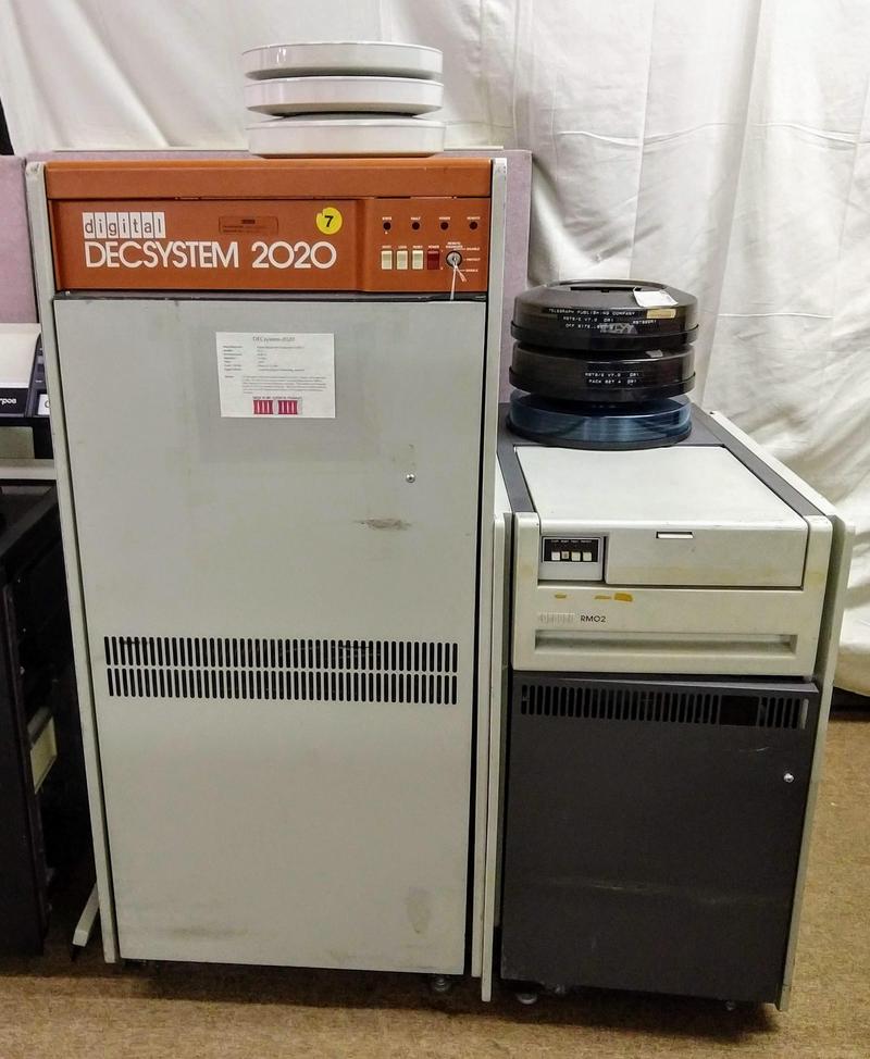
DEC started producing mainframes in 1966 with the PDP-10, a 36-bit computer that popularized time-sharing. The museum has a DECsystem-2020 (1978), the smallest member of the PDP-10 family.

A DECsystem-2020 mainframe next to an RM02 disk drive. The drive's removable disk packs each store 67 megabytes.

A DECsystem-2020 mainframe next to an RM02 disk drive. The drive's removable disk packs each store 67 megabytes.

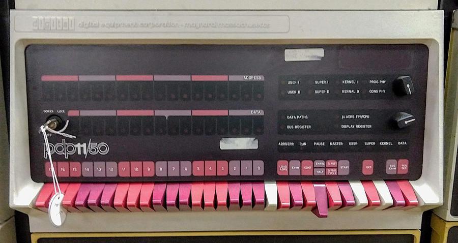
In 1970, DEC introduced the 16-bit PDP-11, which became the most popular minicomputer with about 600,000 sold. The museum has many different PDP-11 models including the PDP-11/05 (1972; photo, console), the fast PDP-11/50 (1972; below, photo), the compact and popular PDP-11/34 (1976; photo), and the PDP-11/44 (1981; photo).

Console of the PDP-11/50 minicomputer.

Console of the PDP-11/50 minicomputer.

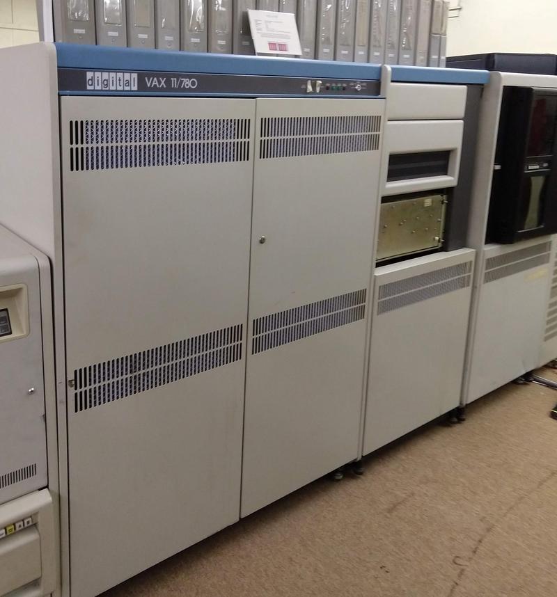
DEC's PDP-11 evolved into the VAX line of 32-bit computers. Larger and more powerful than earlier minicomputers, these systems were known as superminicomputers. The VAX-11/780 (1978; below) was the first member of the VAX family, and was implemented with TTL chips. The museum has a VAX-11/750 (1980) and the cheap single-cabinet VAX-11/730 (1982; photo), the powerful VAX-6000 (1991; photo), and top-of-the-line VAX-7000 (1992; photo). The VAXstation 4000 Model 90 (1991; photo) was a workstation implementing the VAX instruction set.

The VAX 11/780 "superminicomputer".

The VAX 11/780 "superminicomputer".

DEC started struggling in the 1990s as the market shifted to personal computers. DEC was acquired in 1998 by personal computer manufacturer Compaq, which in turn was soon acquired by Hewlett-Packard in 2002.

Other systems

The museum has systems from many other companies such as Varian, Control Data, Wang, Panasonic, Silicon Graphics, Singer, and Tektronix, but I'll just touch on some highlights.

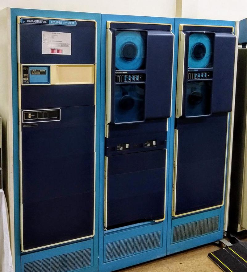
Data General was a major producer of minicomputers, third behind DEC and IBM. The Data General Eclipse was the successor to the popular Data General Nova 16-bit minicomputer. It is represented in the museum by the Eclipse S/280 (1975; below) and Eclipse S/120 (1982; photo). Data General moved into the microcomputer market with the microNOVA (1977; photo), but it wasn't commercially successful.

Data General Eclipse S/280 minicomputer.

Data General Eclipse S/280 minicomputer.

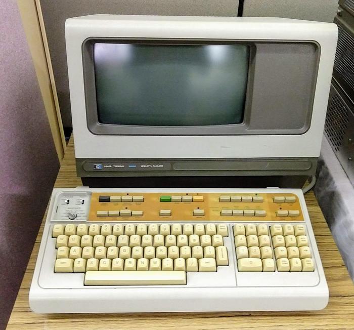
In the late 1970s, Hewlett-Packard was the fourth-largest producer of minicomputers. The HP 2116B minicomputer (1968; photo) was part of the HP 1000 (photo) family of 16-bit minicomputers designed for instrument control and automation. The HP 2645A terminal (below) was part of HP's line of terminals.

HP 2645A terminal

HP 2645A terminal

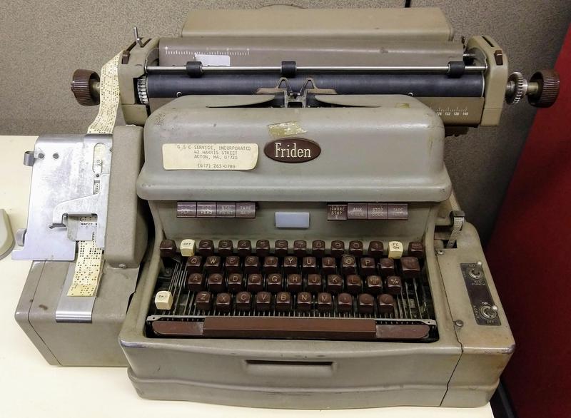
Another interesting terminal is the Friden Flexowriter from the early 1960s (below). It has a paper tape reader and punch on the left. Flexowriters were often used as console terminals for computers.

Friden Flexowriter

Friden Flexowriter

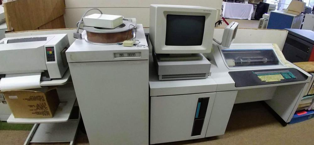
The Burroughs B80 is a multi-user office minicomputer (1978; below). It has as dot-matrix printer above the keyboard. The computer on display was used by a funeral home, and has a paper product list taped above the keyboard with products such as "Tranquility urn", "Open/Close grave", and "Move dirt more than 25 miles".

The Burroughs B80 office minicomputer.

The Burroughs B80 office minicomputer.

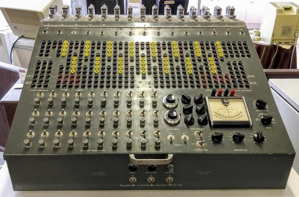
The collection also includes analog computers, such as the Heathkit H-1 (1950s) which used vacuum tube amplifiers and represented values by signals from -100 to 100 volts. It could be programmed to solve differential equations by wiring the patch board. The museum also has a Comdyna GP-6 (photo), a more modern transistorized analog computer from the late 1960s.

A Heathkit H1 analog computer. Vacuum tubes are on top, the plugboard is in the middle, and potentiometer controls are in the front.

A Heathkit H1 analog computer. Vacuum tubes are on top, the plugboard is in the middle, and potentiometer controls are in the front.

Microcomputers in the Large Scale Integration Museum

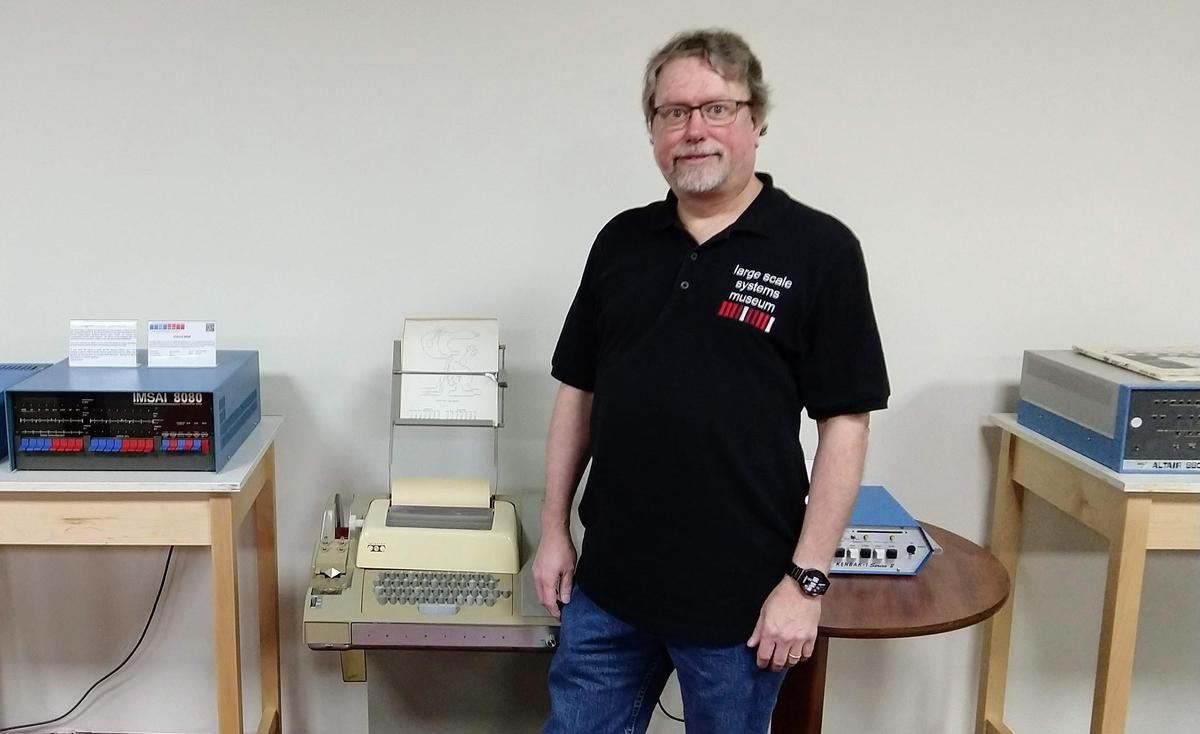
Upstairs is the "Large Scale Integration Museum", a large collection of microcomputers of the 1970s and 1980s. The collection focuses on microcomputers before to the IBM PC and x86 processors. Since I'm more interested in the larger computers, I'll discuss this collection briefly, but I don't want to downplay its impressive scope.

Corey Little, curator of the microcomputer collection, in front of Imsai, ASR-33 teletype, Kenbek-1 replica, and Altair.

Corey Little, curator of the microcomputer collection, in front of Imsai, ASR-33 teletype, Kenbek-1 replica, and Altair.

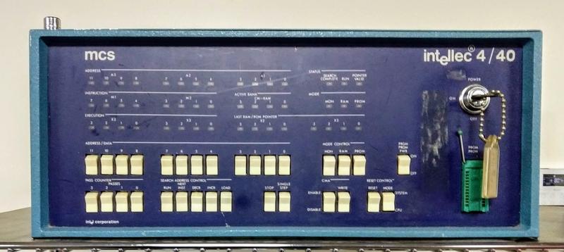
The first commercial microprocessor was Intel's 4-bit 4004, introduced in 1971. The Intel Intellec 4/40 development system (below), used the 4040 microprocessor (1974), an improved version of the 4004. This system was intended for engineers to develop software for embedded systems using the 4040 chip.

Intel Intellec 4/40 development system. An EPROM socket below the key allowed software to be burned into EPROM chips.

Intel Intellec 4/40 development system. An EPROM socket below the key allowed software to be burned into EPROM chips.

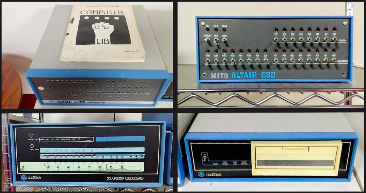
The microcomputer revolution took off when Intel released the 8-bit 8080 microprocessor in 1974, leading to the first commercially successful personal computer, the MITS Altair 8800 kit (1975). In addition to the Altair 8800, the museum has the updated Altair 8800b and the more obscure Altair 680, which uses the Motorola 6800 microprocessor.

Altair 8800 (with the famous manifesto Computer Lib on top), Altair 680, Altair 8800b, and disk drive for Altair.

Altair 8800 (with the famous manifesto Computer Lib on top), Altair 680, Altair 8800b, and disk drive for Altair.

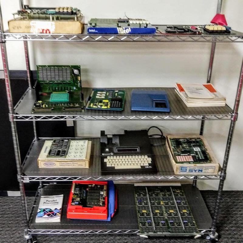
Single-board computers also helped popularize microprocessors. Companies produced development kits for engineers to experiment with new microprocessors and hobbyists often used them due to their low cost. The museum has several racks of these development boards; the rack below includes the Intel SDK-85 System Design Kit for the 8085 microprocessor, Artisan Electronics Model 85 microcalculator (a single-board scientific calculator that could be interfaced to a microcomputer), Rockwell's 6502-based AIM-65, Synertek's 6502-based SYM-1, and Transputer parallel processor boards.

A variety of development boards and single-board computers.

A variety of development boards and single-board computers.

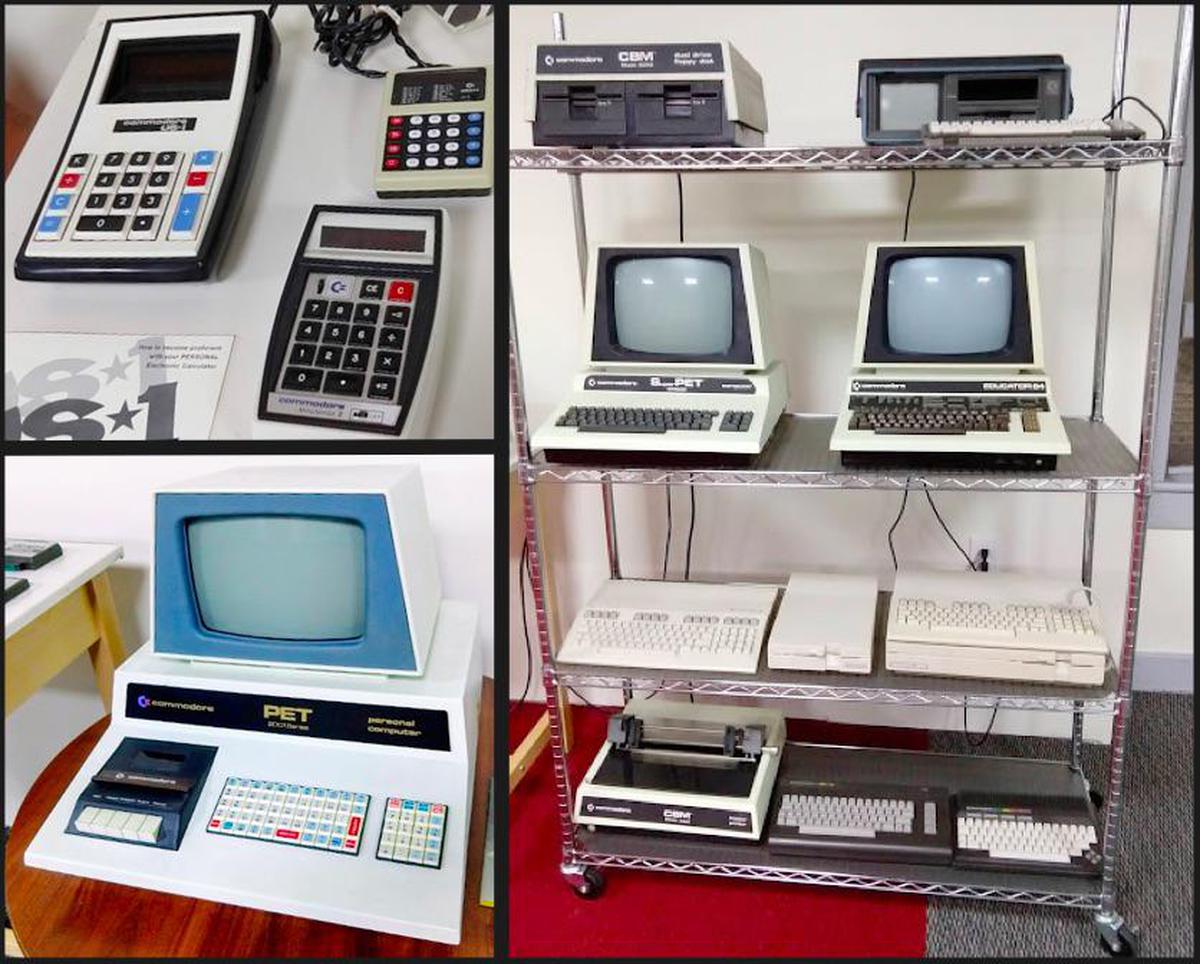
By the late 1970s, microcomputers became mass-market products, with the introduction of home computers that were more affordable and usable by the general public. The museum has many other popular home computers from manufacturers such as Atari, Sinclair, Radio Shack, Heathkit, and Texas Instruments. The photo below shows part of the Commodore collection.

The Commodore collection includes calculators, Commodore Super PET, Educator 64, PET 4032, and PET 2001

The Commodore collection includes calculators, Commodore Super PET, Educator 64, PET 4032, and PET 2001

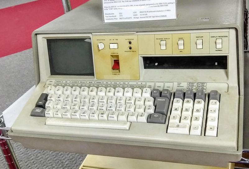
Early portable computers were suitcase-sized and often called luggables. The museum has a large collection including the IBM 5100 (1975; below), Osborne One (1981), Osborne Executive, Osborne Vixen, and Kaypro II, as well as more obscure machines such as the Telcon Zorba and General Electric Workmaster.

The IBM 5100 portable computer was introduced in 1975, six years before the IBM PC. Its keyboard has special characters for the APL language.

The IBM 5100 portable computer was introduced in 1975, six years before the IBM PC. Its keyboard has special characters for the APL language.

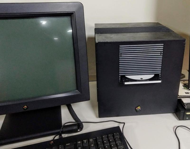
Apple is represented by a variety of Apple II, Apple III, Lisa, and Macintosh systems. The collection also includes a NeXTcube, the workstation developed by Steve Jobs in the 1980s after he was forced out of Apple. Steve Jobs returned to Apple when Apple purchased NeXT in 1997, leading to Apple's dramatic rise. The NeXTcube's operating system led to Apple's current macOS and iOS operating systems.

The NeXTcube workstation was packaged in a 1-foot magnesium cube.

The NeXTcube workstation was packaged in a 1-foot magnesium cube.

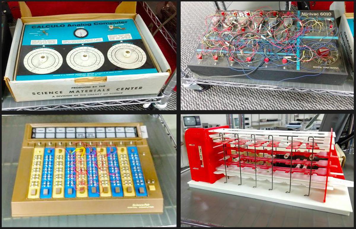
The museum has various toys and educational devices that were produced to explain computers, including the CALCULO Analog Computer (1959), Minivac 6010 (1962) created by the father of information theory Claude Shannon, Radio Shack Science Fair Digital Computer Kit (1977), and Digi-Comp 1 (1963).

The collection includes toy computers such as the CALCULO Analog Computer, MINIVAC 6010, Radio Shack ScienceFair Digital Computer, and Digi-Comp 1.

The collection includes toy computers such as the CALCULO Analog Computer, MINIVAC 6010, Radio Shack ScienceFair Digital Computer, and Digi-Comp 1.

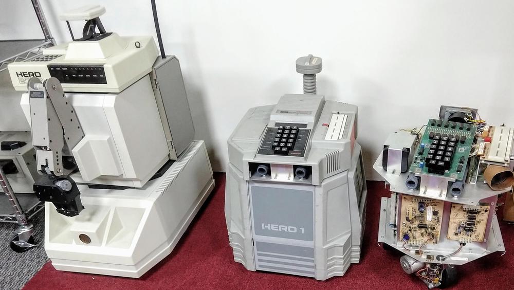
Heathkit introduced the HERO-1 kit robot in 1982, providing a way for hobbyists to experiment with robotics. Nowadays, Arduinos and cheap servos and stepper motors make it easy to build a simple robot, but in 1982, robotics was much more difficult. The HERO-1 kit cost $1500 (equivalent to about $4000 today).

Three Heathkit HERO robots. The HERO 2000 (1986, left) included multiple processors and speech synthesis, while the older HERO-1 robots have a single 6808 processor. The "eyes" are an ultrasonic distance sensor.

Three Heathkit HERO robots. The HERO 2000 (1986, left) included multiple processors and speech synthesis, while the older HERO-1 robots have a single 6808 processor. The "eyes" are an ultrasonic distance sensor.

Conclusion

The Large Scale Systems Museum contains a remarkable collection of large computer systems and microcomputers from the 1970s to 1990s The museum, hidden behind a storefront on a quiet small-town main street, illustrates an interesting period in computer history. During this time, mainframes, minicomputers, and supercomputers reached their peak and then went into steep decline. Meanwhile, the microprocessor passed through the hobbyist phase and the home computer phase before achieving its dominance. Amazingly most of the systems at the museum are up and running, giving the visitor a feel for the computers of that era.

The museum is open by appointment only; details are here and on their Facebook page. If you ever find yourself near New Kensington, PA (half an hour outside Pittsburgh), get in touch with them. I've only presented the highlights of the museum; more photos are here. I announce my latest blog posts on Twitter, so follow me @kenshirriff for future articles. I also have an RSS feed.